Combinational Logic Circuits
Gate Circuits and Boolean Equations
Binary Logic and Gates
Binary Variables 1/0, true/false, on/off
Logical Operations
AND(\(\cdot\))OR(+)NOT(\(\bar A\) or \(A'\) or ~\(A\))XOR
Truth tables a tabular listing of the values of a function for all possible combinations of values on its arguments.
Logic Function Implementation
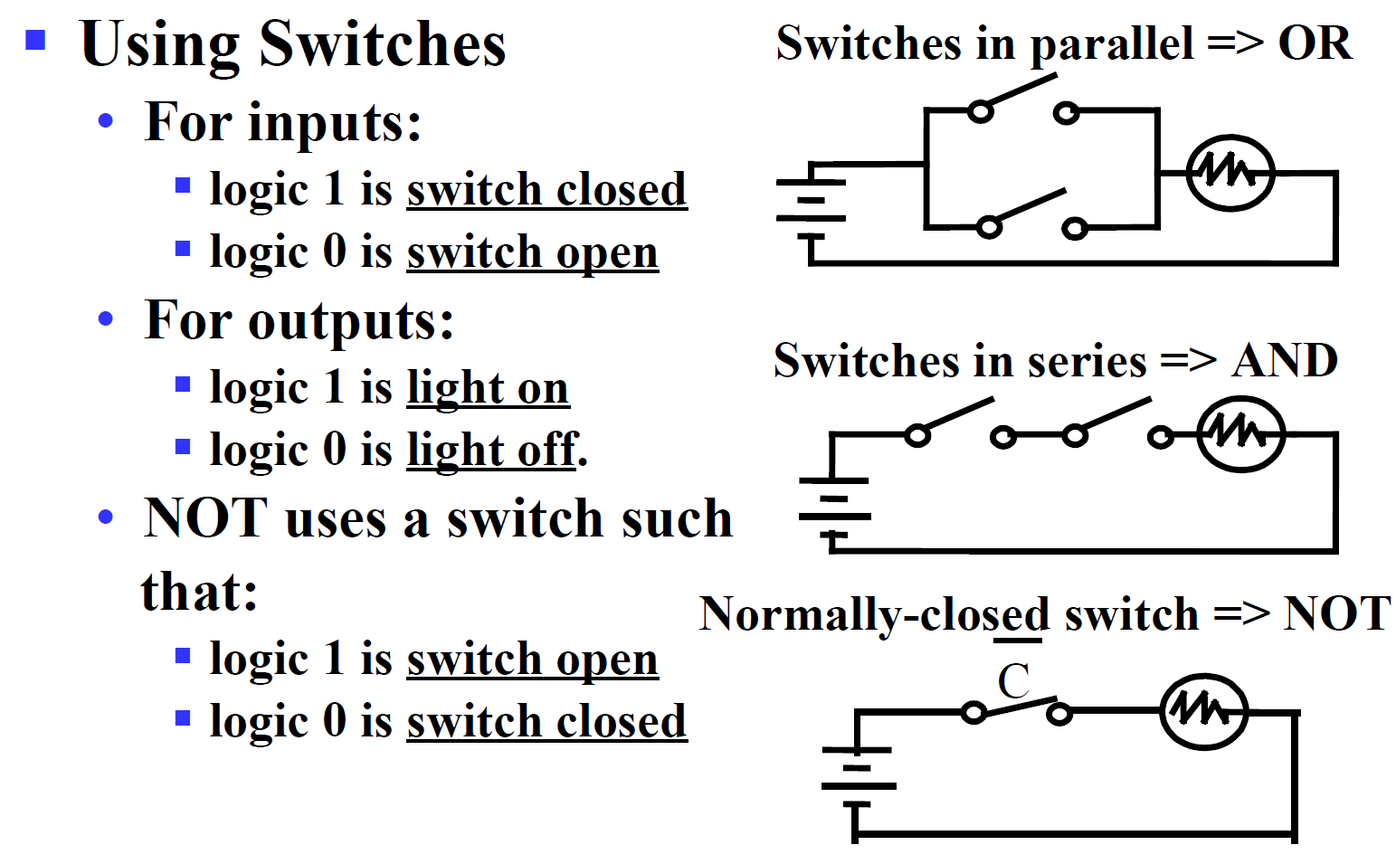
Using Switches 开关电路
Logic Gates
继电器 (relay) 实现开关。不可靠,寿命有限,体积大
电子管 (vacuum rube) 实现开关。需要预热,体积大,寿命有限
半导体 (transistor) 实现开关。
半导体
导电特性处于导体和绝缘体之间。
分类
-
本征半导体
不含杂质且具有晶体结构的半导体
T = 0K 时,不导电
-
杂质半导体
-
N 型半导体 (Negative)
掺入 5 价原子,存在自由电子
-
P 型半导体 (Positive)
掺入 3 价原子,存在电子空缺
-
PN 结
一侧 P 型,一侧 N 型,交界处形成 PN 结,中间电子和空穴结合。
- 外加正向电压(和内部电压相反),PN 结被耗尽后电流导通
- 外加反向电压,PN 结扩大,电流更小。饱和电流随温度升高而变化。
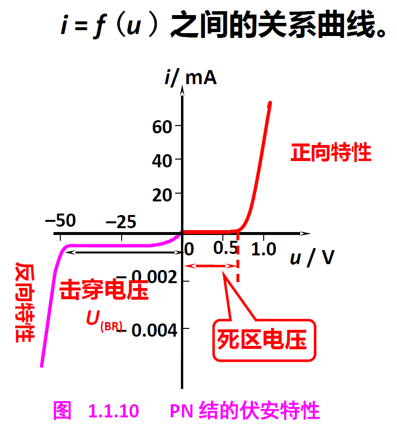
伏安特性曲线:
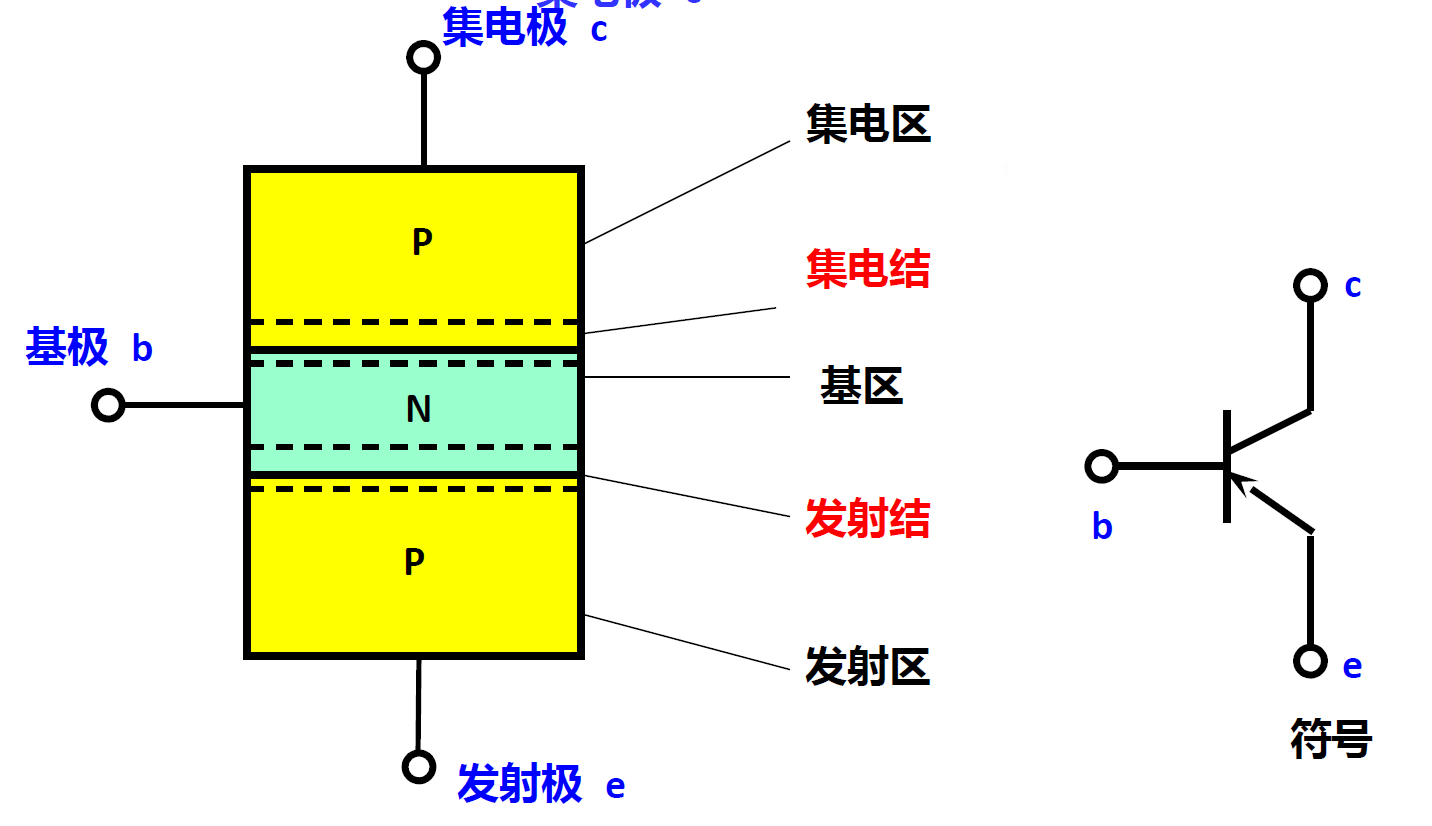
三极管
半导体三极管、晶体三极管。
分类
-
NPN 型
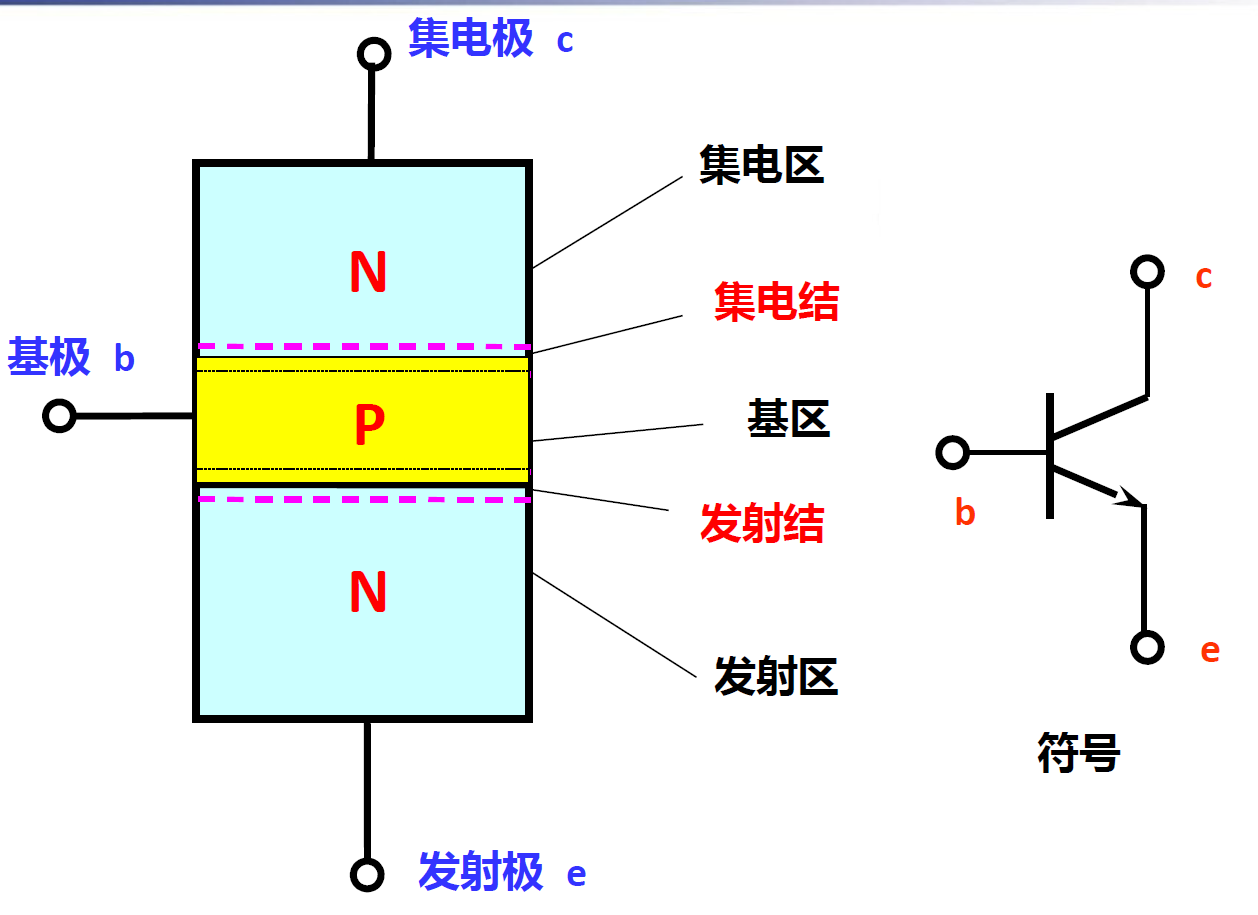
放大特性:\(I_b = \beta I_c\)
可看为又基极控制的开关,基极电流很小看作断开,电流很大看作闭合。
-
PNP 型
CMOS Circuits 电压控制
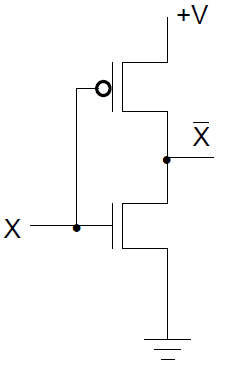
上面 PMOS 管,常闭;下面 NMOS 管,常开。
与非(NAND)和或非(NOR)门(能够构造出所有逻辑关系)
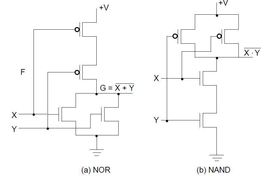
输入段可接在一起,输出端不能接在一起,可能短路。
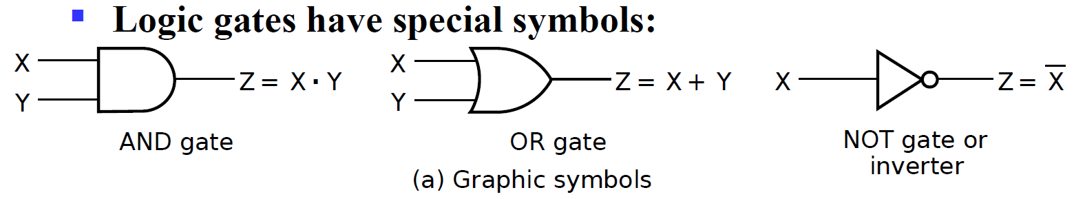
Logical Gate Symbols
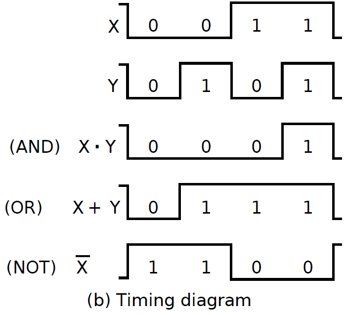
Waveform Behavior in Time
Gate Delay
限制最高工作频率。
Logic Diagrams and Expressions
真值表唯一,逻辑函数和逻辑电路图有很多变形。
Bool Algebra
重点:\(X + YZ = (X + Y)(X + Z)\)
对偶:与变或,或变与,0 变 1 ,优先级不变,非不变。
Boolean Algebraic Proof 1
Boolean Algebraic Proof 2
Boolean Algebraic Proof 3
Useful Theorems
- Minimization: \(x \cdot y + \bar x \cdot y = y, (x + y)(\bar x + y) = y\)
- Absorption: \(x + xy = x, x(x+y) = x\)
- Simplification: \(x + \bar x y = x + y, x(\bar x + y) = xy\)
- Consensus: \(xy + \bar xz + yz = xy + \bar xz\) \((x+y)(\bar x+z)(y+z) = (x+y)(\bar x+z)\)
- DeMorgan's Law: \(\overline{x + y} = \bar x\bar y, \overline{xy} = \bar x + \bar y\)
Expression Simplification 减少延迟,降低成本
Standard Forms
Canonical Forms in common usage:
- SOM: Sum of Minterms
- POM: Product of Maxterm
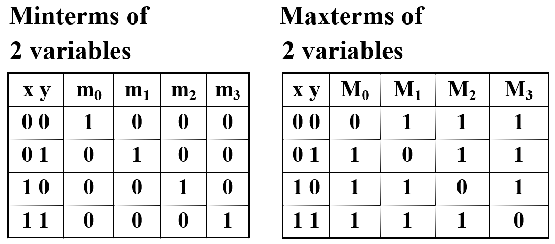
Minterms and Maxterms
- Minterm:
ANDterms with every variable present in either true or complemented form. - Maxterm:
ORterms with every variable in true or complemented form.
Index of minterms and maxterms

The index for the minterm or maxterm, expressed as a binary number, is used to determine whether the variable is shown in the true form or complemented form.
For Minterms:
- "1" means the variable is "Not Complemented" (\(x\))
- "0" means the variable is "Complemented" (\(\bar x\))
For Maxterms, the situation is opposite.
Use subscript to show index and "m" for Minterm, "M" for Maxterm. \(M_i = \bar m_i\).
Function Tables for both
Canonical Forms
Canonical Sum of Minterms
- For the function table, the minterms used are the terms corresponding to the 1's
- For expressions, expand all terms first to explicitly list all minterms. Do this by "ANDing" any term missing a variable v with a term \(v + \bar v\)
Example
Implement \(f = x + \bar x \bar y\) as a SOM.
- \(f = x (y + \bar y) + \bar x \bar y\)
- \(f = xy + x \bar y + \bar x \bar y\)
- \(f = m_3 + m_2 + m_0\) or \(f(x, y, z) = \sum_m(0, 2, 3)\)
Canonical Product of Maxterms
- For the function table, the maxterms used are the terms corresponding to the 0's
- For expressions, expand all terms first to explicitly list all maxterms. Do this by "ORing" any term missing a variable v with a term \(v \bar v\)
Example
Implement \(f = x + \bar x \bar y\) as a POM.
- \(f(x, y, z) = (x + bar x)(x + \bar y) = x + \bar y\)
- \(f = x + \bar y + 0 = x + \bar y + z \bar z\)
- \(f = (x + \bar y + z)(x + \bar y + \bar z)\)
- \(f = M_2 M_3 = \prod_M (2, 3)\)
Function Complements
The complement of a function expressed as a sum of minterms is constructed by selecting the minterms missing in the sum-of-minterms canonical forms.
Minterm 和 Maxterm 在真值表中选择的项互补,可以通过 SOM 推算出 POM。
Note
Method to get maxterm.
先化成 SOM,再选取互补的项算出 POM。
- \(F(x, y, z) = \sum_m(1,3,5,7)\)
- \(F(x,y,z) = \prod_M(0,2,4,6)\)
Standard Forms
- Standard Sum-of-Products (SOP) form: equations are written as an OR of AND terms
- Standard Product-of-Sums (POS) form: equations are written as an AND of OR terms
SOP and POS are two-level network of gates. 一级或门再一级与门(或者相反),最少层次的电路实现方法。
目的:减少延迟、成本。
Circuit Optimization
Goal: To obtain the simplest implementation for a given function.
Requires a cost criterion to measure the simplicity of a circuit.
Two-Level Optimization
Cost criteria:
- \(L\) - Literal cost
- \(G\) - Gate input cost
- \(GN\) - Gate input cost with NOTs
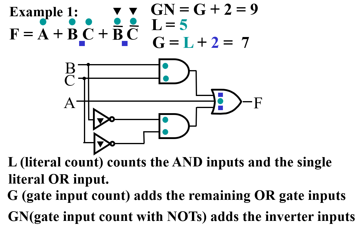
Literal Cost
The number of literal appearances in a Boolean expression corresponding to the logic circuit diagram.
式中变量总个数即为 Literal Cost.
Gate Input Cost
The number of inputs to the gates in the implementation corresponding exactly to the given equation or equations.
Consist of:
- All literal appearances
- The number of terms excluding single literal terms (G)
- Optionally, the number of distinct complemented single literals (GN)
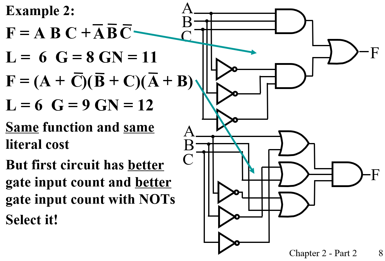
Example
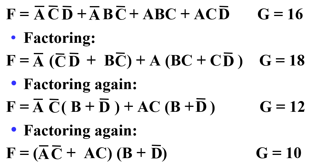
- \(F = BD + A\bar BC + A\bar C \bar D \qquad L = 8, G = 11, GN = 14\)
- \(F = (A +\bar B)(A + D)(B + C + \bar D)(\bar B + \bar C + D) \qquad L = 10, G = 14, GN = 18\)
Cost Criteria
Map Manipulation
Karnaugh Maps(K-map)
A K-map is a collection of squares
- Each square represents a minterm
- The collection of squares is a graphical representation of a Boolean function
- Adjacent squares differ in the value of one variable
- Alternative algebraic expressions for the same function are derived by recognizing patterns of squares
Two Variable Maps

K-Map Function Representation
\(F(x,y) = x\bar y + xy\)

Then \(F(x,y) = x\bar y + xy = x\)
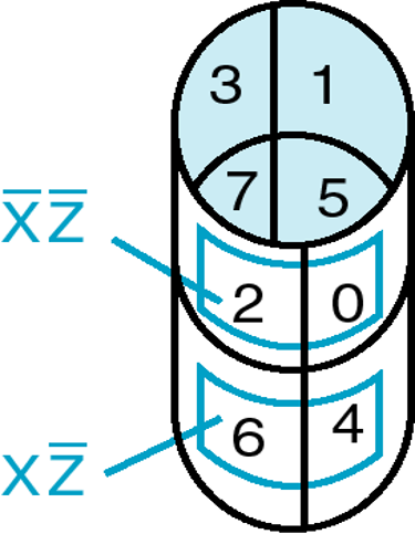
Three Variable Maps
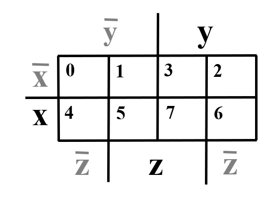
Note
Topological warps of 3-variable K-maps that show all adjacencies:
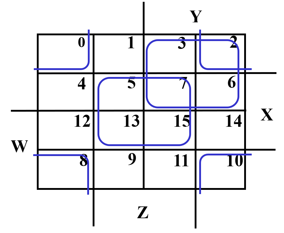
Four Variable Maps
Example Shapes of Rectangles (WXYZ)
Five Variable or More K-Maps
For five variable problems, we use two adjacent K-maps.(VWXYZ)

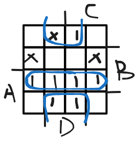
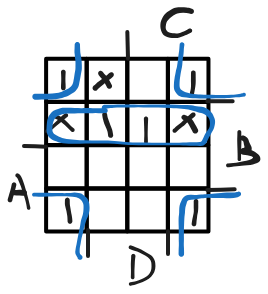
Don't Cares in K-Maps
可能有无关项,输入无关输入组合时,输出是 0 是 1 都无所谓。在 K-map 中用 x 表示,可画入也可不画入卡诺圈中(取决于是否能化到最简)
Example
\(F(A,B,C,D) = \sum_m(3,9,11,12,13,14,15) + \sum_d(1,4,6)\)
- Find the optimum SOP solution
\(F = AB + \bar BD\)
- Find the optimum POS solution
\(F = (B + D)(A + \bar B)\)
Systematic Simplification
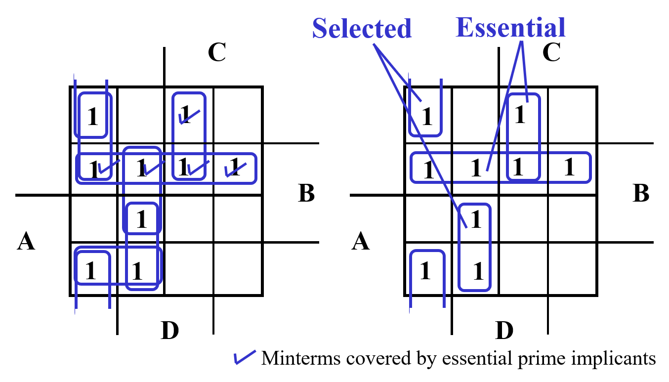
A Prime Implicant (质蕴涵项) is a product term obtained by combining the maximum possible number of adjacent squares in the map into a rectangle with the number of squares a power of 2.
A prime implicant is called an Essential Prime Implicant if it is the only prime implicant that covers (includes) one or more minterms.
质蕴涵项是能够框住某个 1 的最大卡诺圈。对某个 1 而言如果它的质蕴涵项只有一个,那么它是必要的。
Example
Multi-Level Circuit Optimization
二级门传输延迟最小,但门输入成本高。
多级门传输延迟较高,但门输入成本低。
如何设计,取决于需要降低传输延迟还是门输入成本。
Transformation Examples
Additional Gates and Circuits
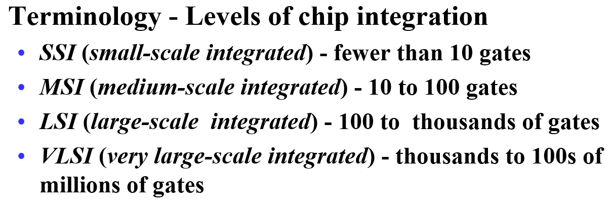
Integrated Circuits
集成电路
Integrated circuit (informally, a “chip”) is a semiconductor crystal (most often silicon) containing the electronic components for the digital gates and storage elements which are interconnected on the chip.
分类:
Technology Parameters
- Fan-in The number of inputs available on a gate
- Fan-out The number of standard loads driven by a gate output
- Logic Levels The signal value ranges for 1 and 0 on the inputs and 1 and 0 on the outputs
- Noise Margin the maximum external noise voltage superimposed on a normal input value that will not cause an undesirable change in the circuit output
- Cost for a gate a measure of the contribution by the gate to the cost of the integrated circuit
- Propagation Delay The time required for a change in the value of a signal to propagate from an input to an output
- Power Dissipation The amount of power drawn from the power supply and consumed by the gate
Fan-out
The number of standard loads driven by a gate output
一个门的输出能带动多少门的输入
衡量扇出系数:
Transition time - the time required for the gate output to change from H to L, \(t_{HL}\), or from L to H, \(t_{LH}\)
带的门越多,上升事件就越长。规定上升下降最大时间,从而得出 maximum fan-out 最大扇出系数。
Cost
In integrated circuits, chip area, number and size of the transistors, amount of wiring, gate input count
主要由门输入成本决定。
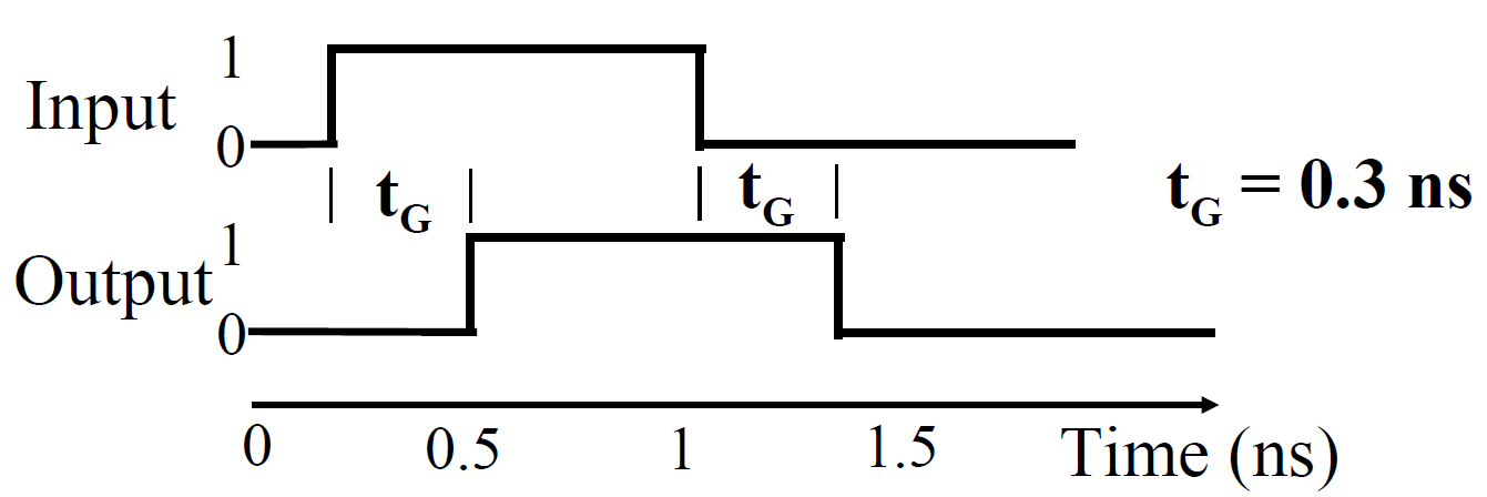
Propagation Delay
Delay is usually measured at the 50% point with respect to the H and L output voltage levels
输入变化到输出变化的时间。通常从上升或下降 50% 处开始计算。
- High-to-Low \(t_{PHL}\) 输出 从高电平到低电平的时间
- Low-to-High \(t_{PLH}\) 输出 从低电平到高电平的时间
Propagation Delay of NOT

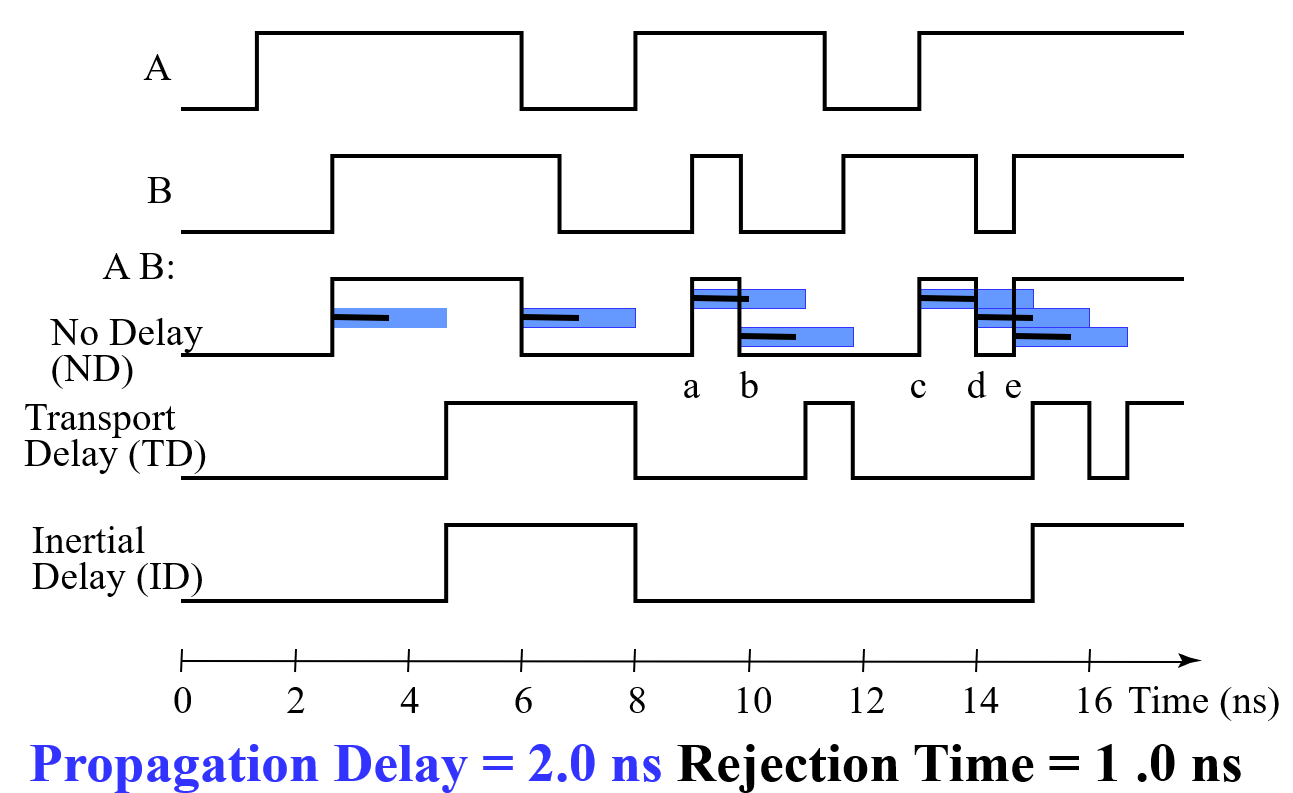
Delay Models
- Transport delay 传输延迟 change in the output in response to a change on the inputs occurs after a fixed specified delay
-
Inertial delay 惯性延迟 similar to transport delay, except that if the input changes such that the output is to change twice in a time interval less than the rejection time, the output changes do not occur. Models typical electronic circuit behavior, namely, rejects narrow “pulses” on the outputs
很小的脉冲跳变会被消除。
Example
Circuit Delay
Example
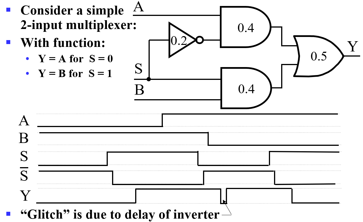
\(S\) 的两条路径延迟不同,\(Y\) 处产生尖峰,称为电路进行的 竞争冒险
Fan-out and Delay
The fan-out loading a gate’s output affects the gate’s propagation delay
standard load: 带一个非门所需要的负载。
Example
One realistic equation for \(t_{pd}\) for a NAND gate with 4 inputs is
\(SL\): the number of standard loads the gate is driving.
Cost/Performance Tradeoffs
Gate-Level Example
NAND gate G with 20 standard loads on its output has a delay of 0.45 ns and has a normalized cost of 2.0.
A buffer H has a normalized cost of 1.5. The NAND gate driving the buffer with 20 standard loads gives a total delay of 0.33 ns.
In which if the following cases should the buffer be added?
- The cost of this portion of the circuit cannot be more than 2.5
- The delay of this portion of the circuit cannot be more than 0.40 ns
- The delay of this portion of the circuit must be less than 0.40 ns and the cost less than 3.0
Answer:
- No buffer
- Need buffer
- Cannot achieve by using buffer or not
Tradeoffs can also be accomplished much higher in the design hierarchy.
Constraints on cost and performance have a major role in making tradeoffs.
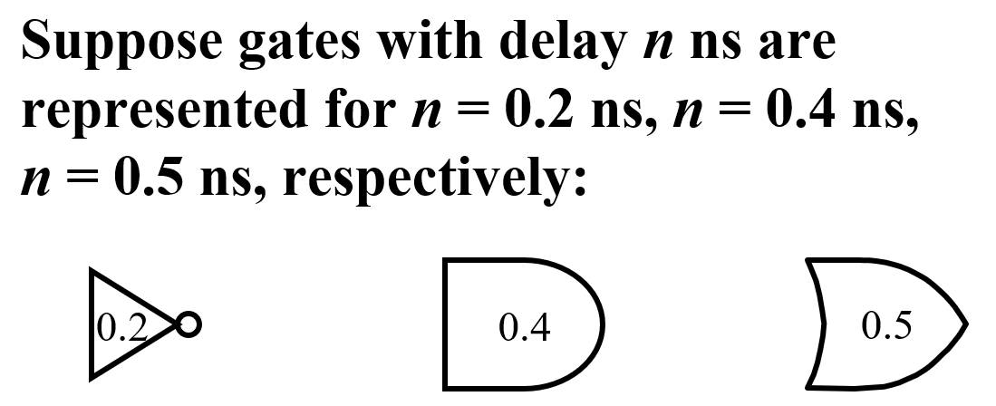
Other Gate Types
-
Buffer 缓冲器 \(F = X\)
作用:扩大扇出系数,减少传输延迟,提高负载能力。
-
NAND gate 与非门 \(F = \overline{XY}\)
作用:实现任意逻辑函数,减少门输入成本。
-
NOR gate 或非门 \(F = \overline{X + Y}\)
对偶关系
-
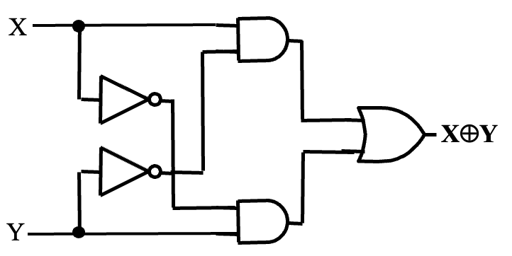
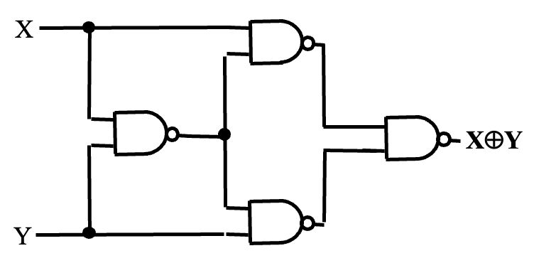
Exclusive-OR gate 异或门 \(F = X \oplus Y\)
Exclusive-NOR gate 异或非门(同或门) \(F = \overline{X \oplus Y}\)
\(X \oplus Y = X \bar{Y} + \bar{X}Y\), \(\overline{X \oplus Y} = XY + \bar{X}\bar{Y}\)
Exclusive-OR Operator and Gates
-
XOR identities
\[ X \oplus Y \oplus Z = \bar X \bar Y Z + \bar X Y \bar Z + X \bar Y \bar Z + XYZ \]\[ X \oplus \bar Y = \overline{X \oplus Y} \]\[ X \oplus 0 = X, X \oplus 1 = \bar X \text{(可控非门)} \] -
XOR implementation
-
Odd and Even Functions
Odd Function: \(F = 1\) if and only if the index of the minterm has an odd number of 1s
Even Function: \(F = 1\) if and only if the index of the minterm has an even number of 1s
The not of an odd function is an even function, and vice versa.
-
Parity Generators and Checkers 奇偶校验
Parity Generator: \(P = X \oplus Y \oplus Z\)
Parity Checker: \(F = X \oplus Y \oplus Z \oplus P\)
High-Impedance Outputs
到 VCC 和 GND 的电阻都很大,相当于断路。简称 Hi-Z。
The 3-State Buffer 真值表:
| Enable | Input | Output |
|---|---|---|
| 0 | X | Hi-Z |
| 1 | 0 | 0 |
| 1 | 1 | 1 |