Combinational Logic Design
Combinational Logic
Functions and Functional Blocks
verilog 中,调用模块会在电路中增加实例,会增加开销。
verilog 中并行运行。
Multiple-bit Rudiementary Functions
A wide line is used to represent a bus (总线). The bus can be split into individual lines.
Enable Function
与门 + 非门

Decoding 译码
the conversion of an n-bit input code to an m-bit output code with \(n \leq m \leq 2^n\) such that each valid code word produces a unique output code
Example:
-
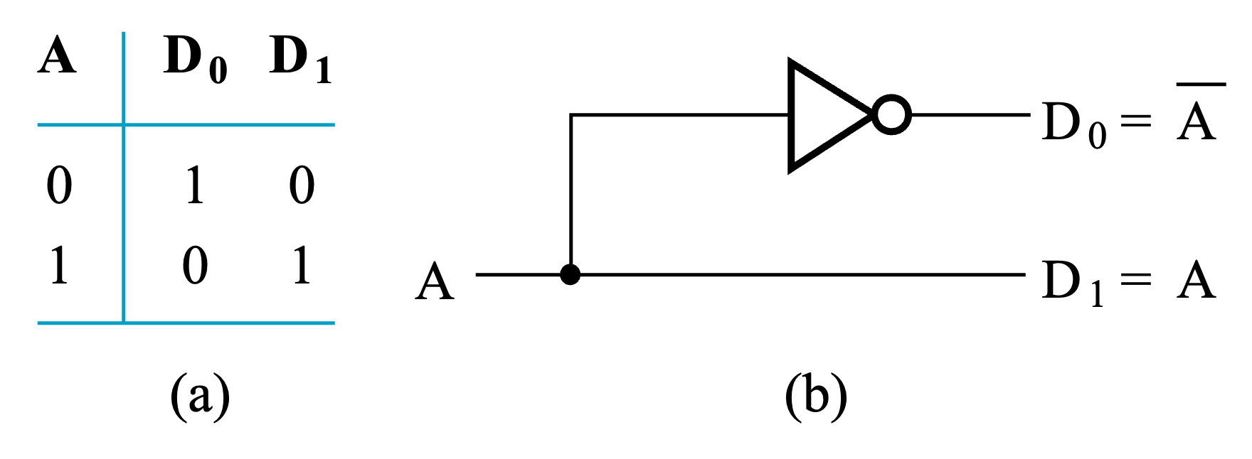
1-to-2-line decoder
-
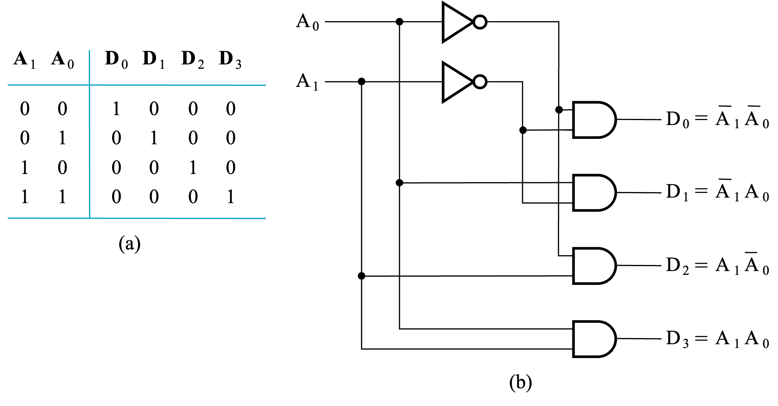
2-to-4-line decoder
行列译码器:将输入不断二分,例如 4-to-16 拆成 2-to4 和 2-to-4,再将 2-to-4 拆成 1-to-2 和 1-to-2。
Logic Functions Implementation
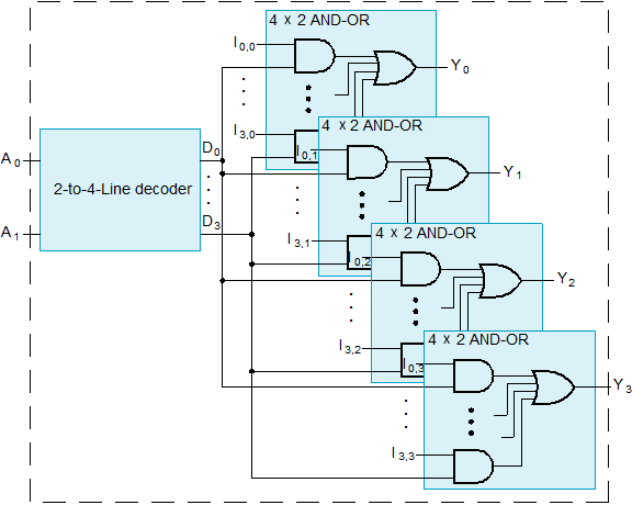
实现任意逻辑函数:译码器 + 或门
译码器输出是所有最小项,通过或门实现逻辑函数。
BCD-to-Segment Decoder
Implement:
-
Common anode 共阳极:
- 控制亮:LED 另一级接低电平(0)
- 控制灭:LED 另一级接高电平(1)
-
Common cathode 共阴极
- 控制亮:LED 另一级接高电平(1)
- 控制灭:LED 另一级接低电平(0)
Encoding 编码
the conversion of an m-bit input code to an n-bit output code with \(m \geq n\) such that each valid code word produces a unique output code (index to code)
Decimal-to-BCD Encoder
- Input: 10 bits (0-9)
- Output: 4 bits (0000-1001)
- Function: if input bit \(D_i\) is 1, then output \((A_3, A_2, A_1, A_0)\) is the BCD code for \(i\).
Commonly don't use truth table.
Equations:
Priority Encoder
Accepts multiple inputs and use the highest priority input.

where \(V\) indicates at least one 1 present.
Use K-map to get equations:
Multiplexers 多路选择器
A multiplexer selects information from an input line and directs the information to an output line.
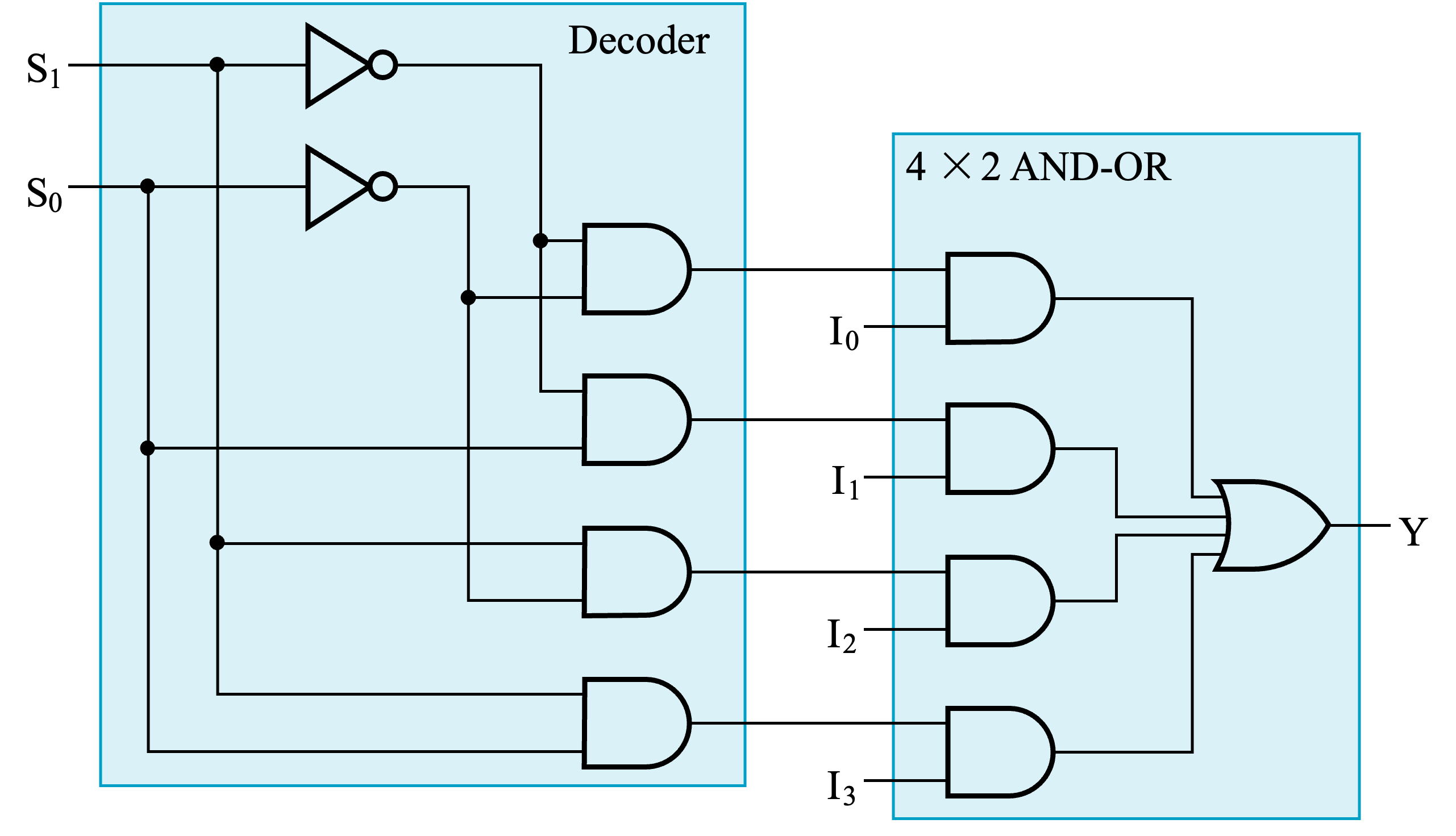
Decoder + Enable.
2-to-1-line Multiplexer
4-to-1-line Multiplexer
Multiplexer Width Expansion
Select "vector bits" instead of "bits".
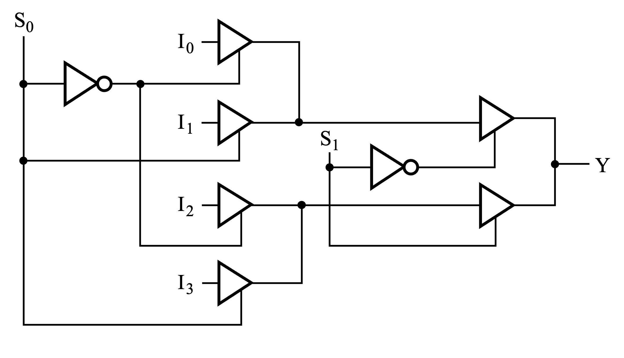
Other Multiplexers
Use three-state drivers.
Combinational Logic Implementation
Multiplexer Approach 1
n inputs, m outputs
Use m-width \(2^n\)-to-1-line multiplexer
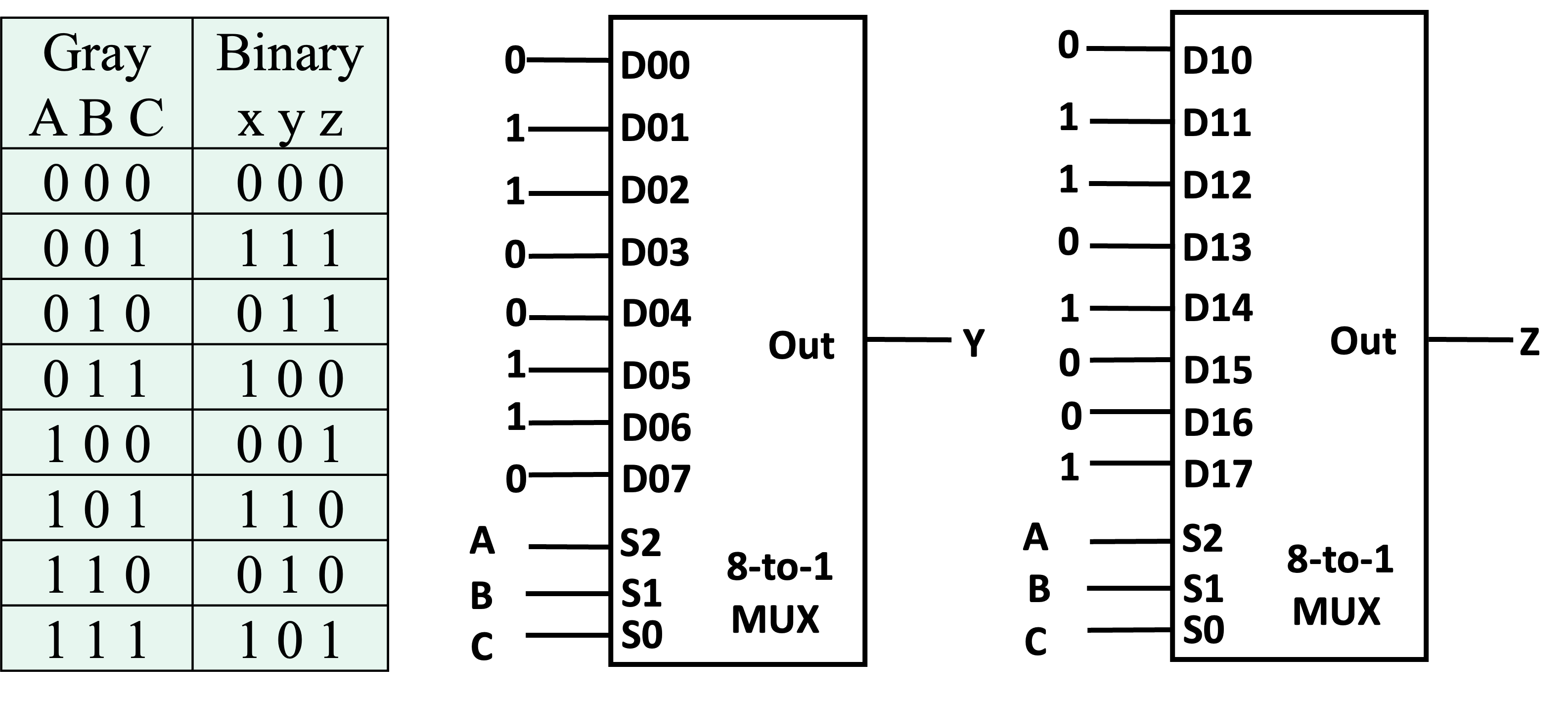
Gray to Binary Code
-
Truth table:

-
Mux:
Multiplexer Approach 2
n + 1 inputs, m outputs
Use m-width \(2^n\)-to-1-line multiplexer.
Design:
- Find the truth table for the function.
- Based on the values of the first n variables, separate the truth table rows into pairs. 根据前 n 个变量的值,将真值表分成两行一对。
- For each pair and output, define a rudimentary function of the final variable \((0, 1, X, \bar X)\)
- Use the first n variables as the select inputs of a multiplexer and the rudimentary functions as the data inputs.
Gray to Binary Code
-
Truth table:
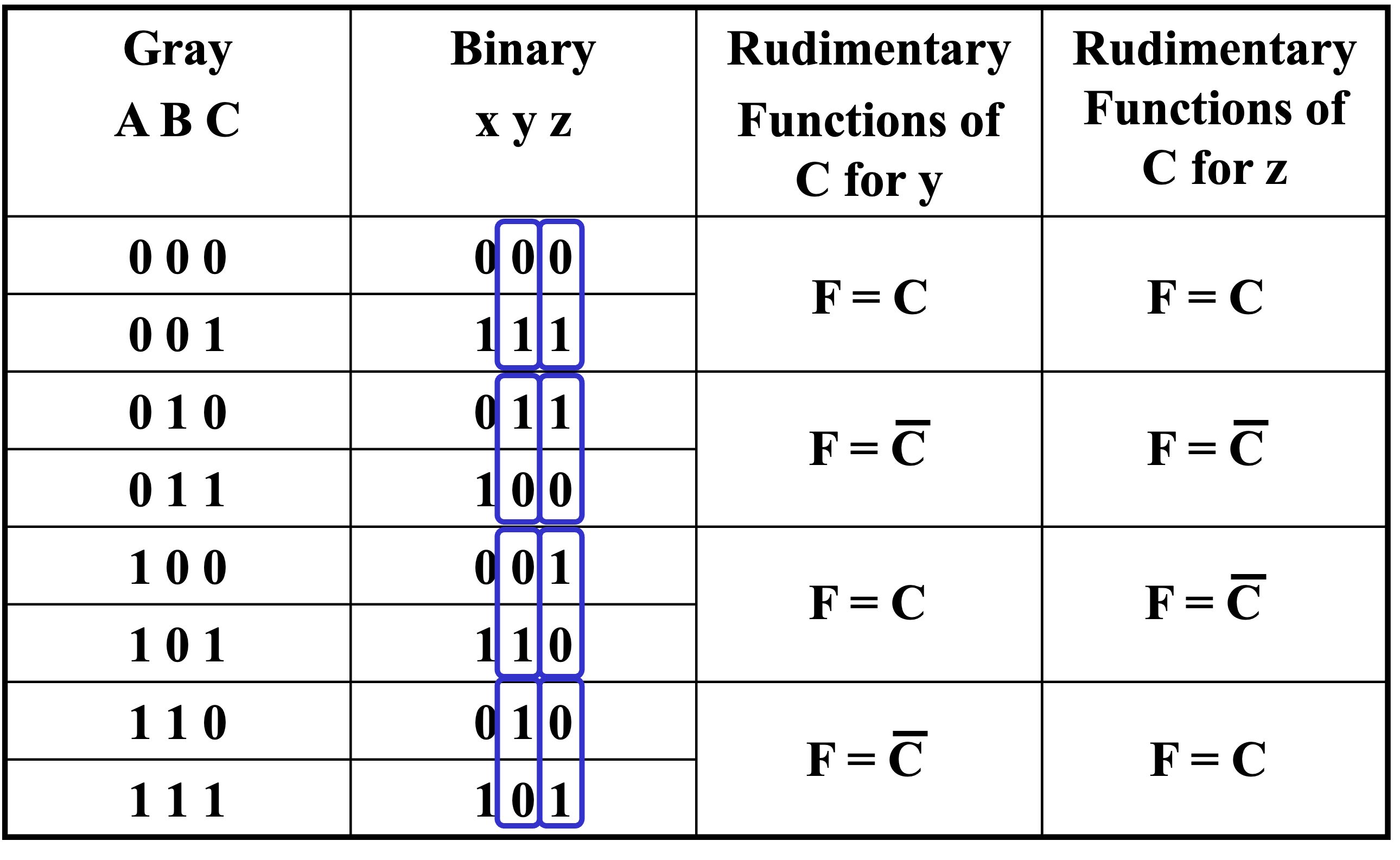
-
Mux:

Design Procedure
Combinational Circuits
输入与输出严格对应
Beginning Hierarchical Design
- Top-Down: 从顶层开始设计,逐步细化
- Bottom-Up: 从最底层开始设计,逐步合并
Design Procedure
- Specification 简化
-
Formulation 公式化
Derive a truth table or initial Boolean equations for each output function.
Apply hierarchical design to the output functions.
-
Optimization 优化
Apply multiple-level logic optimization to the output functions.
Draw logic diagrams.
-
Technology Mapping 技术映射
Map the logic diagrams into a specific technology.
-
Verification 验证
Verify the design by simulation.
Design BCD to Excess-3 Code Converter
-
Specification
- BCD code words for digits 0 through 9 are 0000 through 1001, respectively.
- Excess-3 code words for digits 0 through 9 consisting of 3 added to the BCD code words.
-
Formulation
write truth table (A-F 无关项)
Input BCD: ABCD, Output Excess-3: WXYZ
-
Optimization
-
Use K-maps:
\[\begin{align} W &= A + BC + BD \\ X &= \bar BC + \bar BD + B\bar C\bar D \\ Y &= CD + \bar C \bar D \\ Z &= \bar D \end{align}\]G = 23
-
Multiple-level logic optimization
\(T_1 = C + D\), then
\[\begin{align} T_1 = C + D , G &&= 2 \\ \bar T_1 , G &&= 1 \\ W &= A + B(T_1) , G &&= 4 \\ X &= \bar B(T_1) + B\bar T_1 , G &&= 6 \\ Y &= CD + \bar T_1 , G &&= 4 \\ Z &= \bar D, G &&= 0 \end{align}\]G = 17
-
Technology mapping
Convert to NAND gates or NOR gates.
-
Chip Design Styles
-
Full custom: 为特定应用设计
优点:最小面积,最快速度,生产成本低
缺点:设计周期长,设计成本高
-
Standard cell: 包含标准模块(类似标准库)
优点:设计周期短,设计成本低
缺点:面积大,速度慢,生产成本高
-
Gate array: 门阵列(可编程)
优点:成本最低
缺点:面积大,速度慢
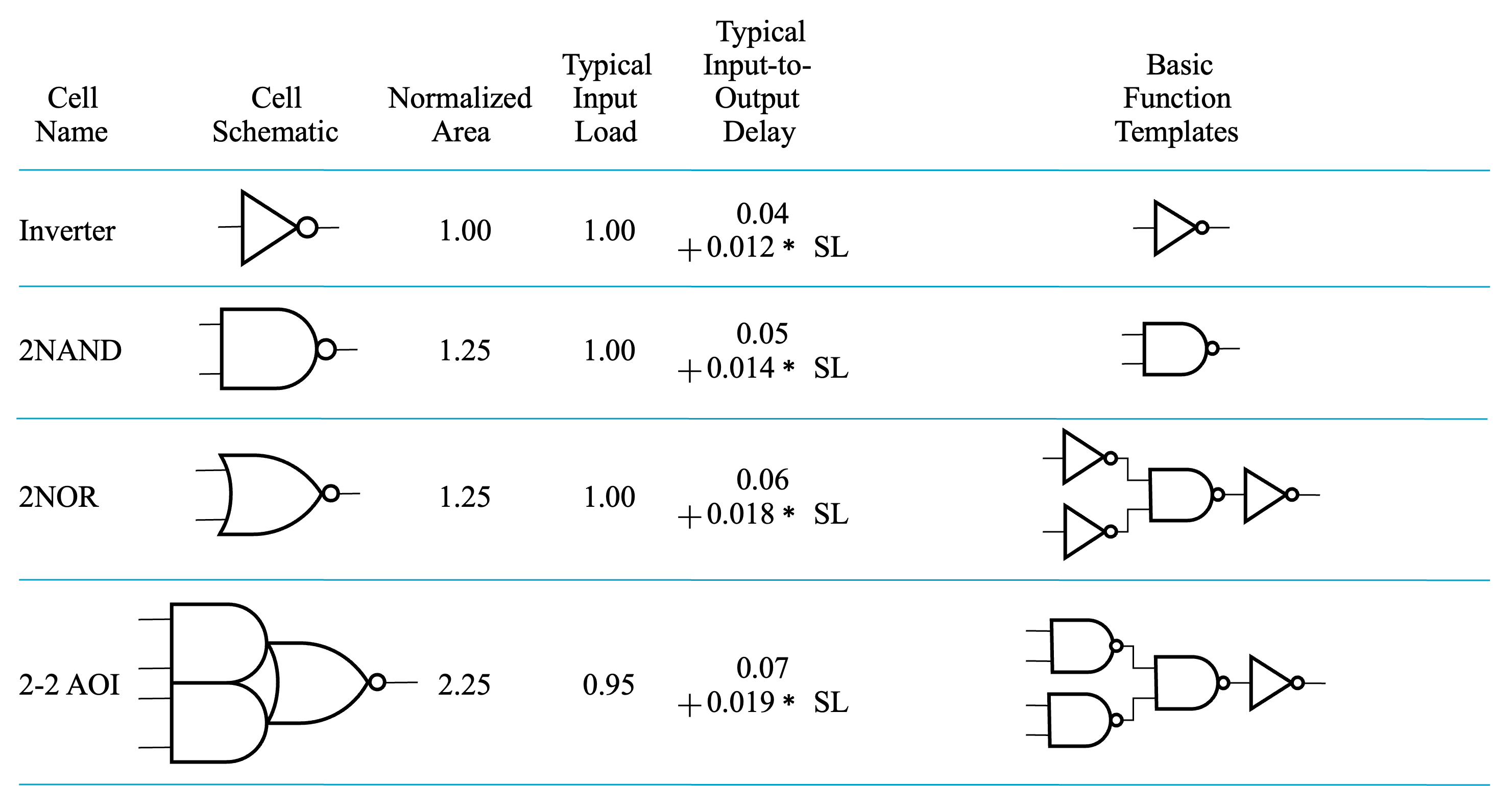
Cell Libraries
- Cell: pre-designed logic block
- Cell library: a collection of cells
- Cell characterization: a detailed specification of the cell for use.
Cell Library
Mapping to NAND gate
Convert any circuits to NAND gates.
Assumptions
- Gate loading and delay are ignored.
- 可以用任意多输入的 NAND 门
-
Convert AND and OR gates to NAND gates
- \(A + B = \overline{\overline{A + B}} = \overline{\bar A \bar B}\)
- \(AB = \overline{\overline{AB}}\)
-
Pushing inverters through circuit fan-out points
Mapping to NOR is similar.
Verificaiton
-
Manual Logic Analysis (Simple Circuits)
- Write a truth table.
- Derive Boolean equations.
-
Simulation
- Write a test program.
- Simulate the circuit.
apply all possible input combinations or important input combinations
Arithmetic Functions
Iterative Combinational Circuits
Use blocked diagram to process each bit.
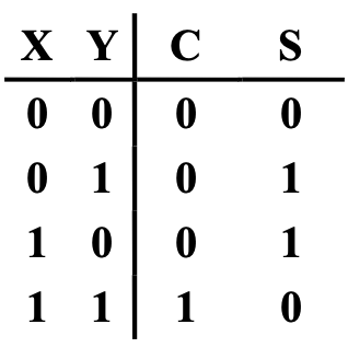
Half Adder
inputs: \(X, Y\); outputs: \(S, C\) (sum, carry)
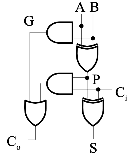
Full Adder
inputs: \(X, Y, Z\) (\(Z\): carry); outputs: \(S, C\)
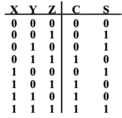
Implement:
4-bit Ripple-Carry Adder
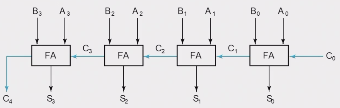
缺点:延迟高(Carry 需要传递)
Carry Lookahead
\(P_i = X_i \oplus Y_i, G_i = X_iY_i\)
\(C_4 = G_3 + P_3G_2 + P_3P_2G_1 + P_3P_2P_1G_0 + P_3P_2P_1P_0C_0\)
缺点:门输入成本大、扇出系数大导致延迟高,随着位数增加,成本大大增加
Group Carry Lookahead Logic
16-bit adder: 4 groups
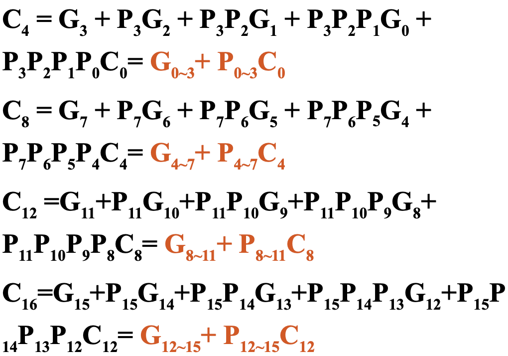
CLA: input \(G_0, P_0, G_1, P_1, G_2, P_2, G_3, P_3\), output \(G_{0\sim 3}, P_{0\sim 3}\)
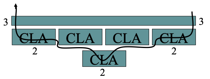
第一层最右 CLA: input \(G_0, P_0, G_1, P_1, G_2, P_2, G_3, P_3\), output \(G_{0\sim 3}, P_{0\sim 3}\)
第二层 CLA: input \(C_0, G_{0\sim 3}, P_{0\sim 3}, G_{4\sim 7}, P_{4\sim 7}, G_{8\sim 11}, P_{8\sim 11}, G_{12\sim 15}, P_{12\sim 15}\), output \(C_4, C_8, C_{12}, C_{16}\)
Longest Delays:
\(A_0, B_0 \to CLA \to G_0, P_0 \to CLA \to C_{12} \to CLA \to C_{16}\)
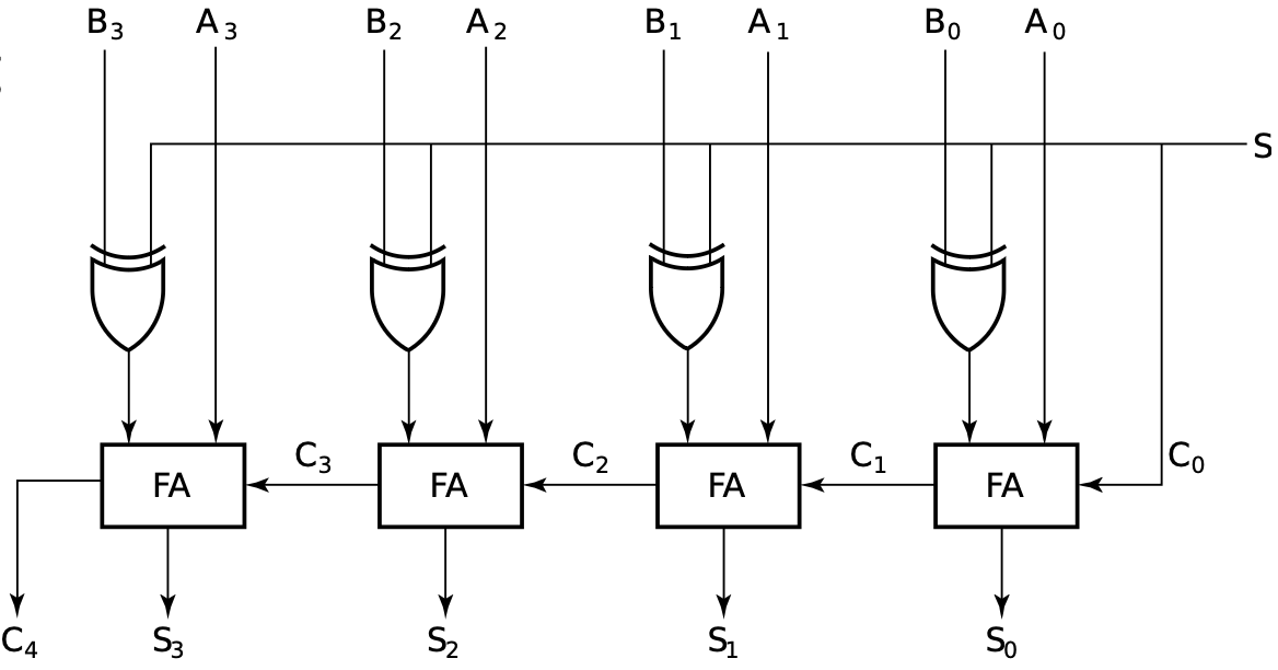
Unsigned Subtraction
Note
compute: \(N - M\)
- \(N \geq M\): 无借位
- \(N < M\): \(N - M = -(2^n - (M - N))\) 最高位借位
一般不用这种方法。
2's Complements:
- Diminished Radix Complement (DRC) 反码 \(2^n - M - 1\)
- Radix Complement (RC) 补码 \(2^n - M\)
\(M - N = M + (2^n - N)\) (n-bit)
- \(M \geq N\): \(2^n\) 溢出,\(M - N\) 保留
- \(M < N\): 结果为负数,求得补码。
如果有进位,则说明结果为正数,无借位;否则结果为负数,有借位。
Signed Integer
最高位是符号位,0 表示正数,1 表示负数。一般采用 2's Complements 即符号位+补码。
电路中的实现
- 加法:直接相加
- 减法:将减数取反加一(变为减数取反之后的补码),再与被减数相加
Overflow Detection
通过符号位判断溢出,有 8 种情况:
-
无溢出
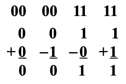
-
有溢出
(注:减负数相当于加正数,\(C_{n-1}\) 为 0;加负数相当于减正数,\(C_{n-1}\) 为 1)
得到溢出判断公式:\(V = C_{n-1} \oplus C_{n}\),这里 \(C_{n}\) 为结果的符号位。
Other Arithmetic Functions
-
Incrementer
- Adding a fixed value to an arithmetic variable
- fixec value = 1, called counting up
- Functional block is called an incrementer
-
Decrementer
- Subtracting a fixed value from an arithmetic variable
- fixec value = 1, called counting down
- Functional block is called a decrementer
-
Multiplier by a Constant: shift left
- Divider by a Constant: shift right
-
Zero Fill and Extension
- Zero fill: add 0s to the MSB or LSB
- Extension: add 0s or 1s to the MSB to extend the length of the variable (usually copy the sign bit)
A + 1 Incrementer
Arithmetic Logic Unit (ALU)
Decompose the arithmetic circuit into:
- An n-bit parallel adder
- A block of logic that selects four choices for the B input of the adder