Sequential Circuits
Storage Elements and Analysis
Introduction to Sequential Circuits
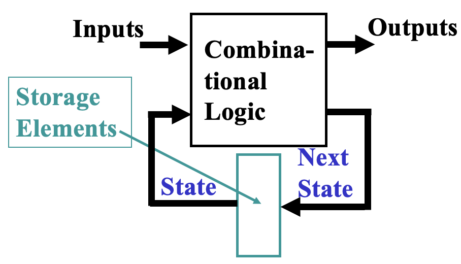
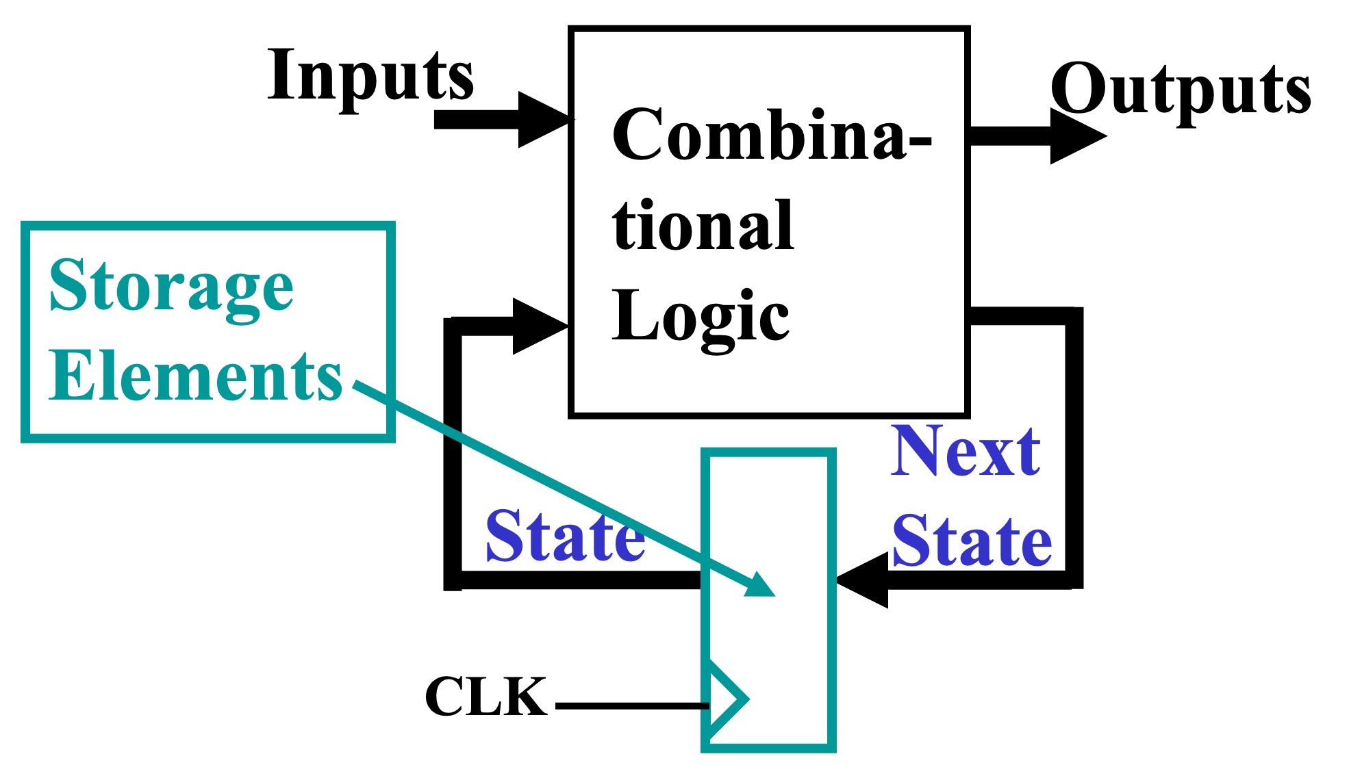
A Sequential circuit contains:
- Storage elements: Latches or Flip-Flops
-
Combinational Logic:
- Implements a multiple-output switching function
- Inputs are signals from the outside.
- Outputs are signals to the outside.
- Other inputs, State or Present State, are signals from storage elements.
- The remaining outputs, Next State are inputs to storage elements.
Combinatorial Logic:
- Next state function 次态方程: Next State = f(Inputs, State)
- Output function (Mealy 模型): Outputs = g(Inputs, State)
- Output function (Moore 模型): Outputs = h(State)
Output function type depends on specification and affects the design significantly
Types of Sequential Circuits
-
Synchronous 同步
- Behavior defined from knowledge of its signals at discrete instances of time
- Storage elements observe inputs and can change state only in relation to a timing signal (clock pulses from a clock)
所有元件同步更新,在时钟周期内更新。有利于分析和设计。
-
Asynchronous 异步
- Behavior defined from knowledge of inputs an any instant of time and the order in continuous time in which inputs change
- If clock just regarded as another input, all circuits are asynchronous. 如果时钟也被看做一个输入,那么所有电路都是 Asynchronous
状态更新可以在任意时间发生。可以有需要的时候更新电路,降低电路的功耗。
Discrete Event Simulation 离散事件仿真
In order to understand the time behavior of a sequential circuit.
Gates modeled by an ideal (instantaneous) function and a fixed gate delay. 所有门的延迟都是固定的,抽象成理想电路门和固定延迟。
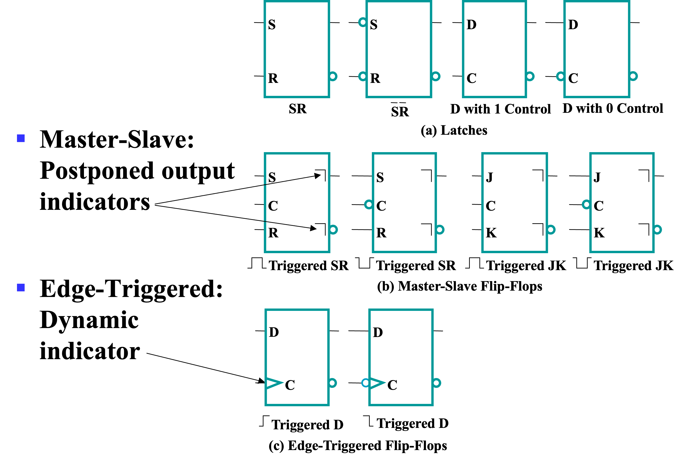
Latch
Basic (NAND) SR Latch


当 \(S = R = 1\) 时,锁存器将保持原来的状态。
当 \(S = 0, R = 0\) 时,锁存器的状态未定义。
其余组合,有 \(Q = \bar S\)。
这种实现被称作 \(\bar S-\bar R\) latch。
Basic (NOR) SR Latch


和 NAND SR Latch 相反。
Clocked SR Latch

当 \(C = 0\) 时,锁存器保持原来的状态,即后面的 \(\bar S-\bar R\) latch 处于锁定状态。
当 \(C = 1\) 时,锁存器的状态由 SR latch 决定。
D Latch

消除了不确定状态,\(C\) 控制锁存,\(D\) 控制输出。\(C = 1\) 时 \(Q = D\)。
Info
在算门输入成本的时候,我们要分开算 G 和 GN. 因为锁存器同时为我们提供了 \(Q\) 和 \(\bar Q\),锁存器可以为后面的组合电路提供原变量和反变量。
The Latch Timing Problem
For a clocked D-latch, the output Q depends on the input D whenever the clock input C has value 1.
锁存器无法做到一个时钟周期内只更新一次。
解决方法:将锁存器的输入和输出分开,使输入不能直接作用在输出上。
Flip-Flops
SR Master-Slave Flip-Flop

前面的锁存器称为 Master,后面的锁存器称为 Slave。
当 \(C = 0\) 时,Master 锁存器不变。
当 \(C = 1\) 时,Master 锁存器的状态由 SR latch 决定,Slave 锁存器被锁定。
当 \(C\) 从 1 变为 0 时,Master 锁存器的状态被锁定,Slave 锁存器的输入接收 Master 锁存器的输出,状态被改变。
1s catching 一次性采样问题
当 \(C = 1\) 时,若 \(S,R\) 出现小扰动,但是在 \(C\) 变为 0 之前恢复,那么 \(Q\) 的状态将会被改变。
解决方法:Use edge-triggering instead of master-slave 使用边沿触发代替主从锁存器。
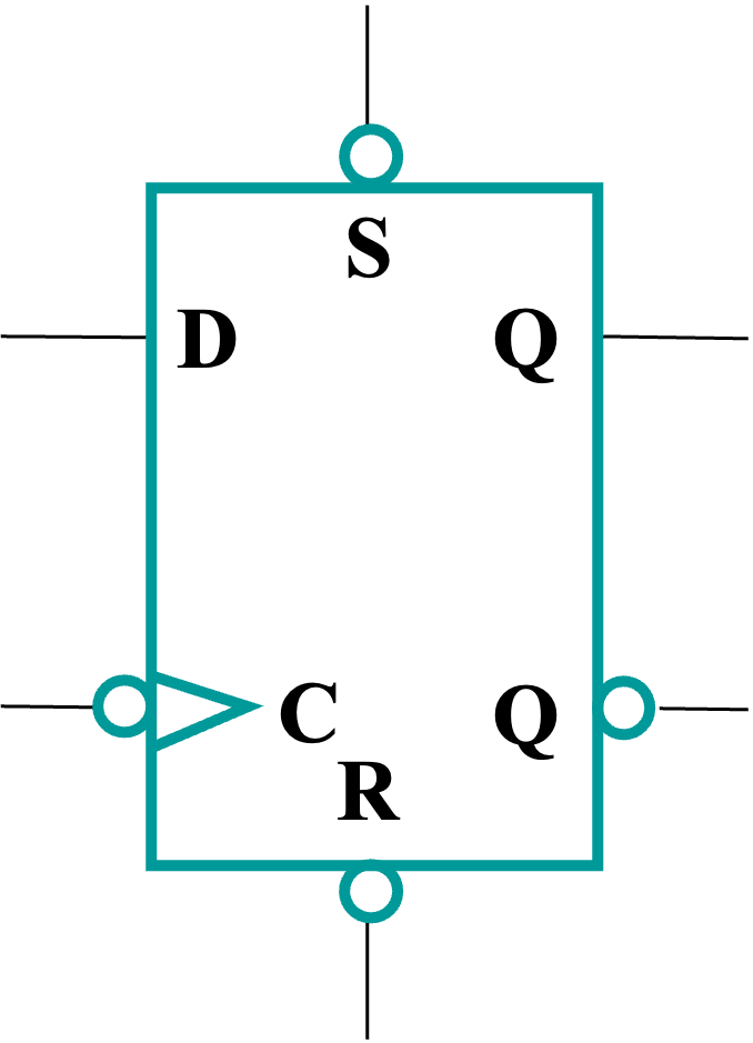
Edge-Triggered D Flip-Flop

The delay of the S-R master-slave flip-flop can be avoided since the 1s-catching behavior is not present with D replacing S and R inputs.
It is called a negative-edge triggered flip-flop, 负边沿触发器。
同样有正边沿触发器:

Actual Circuit of Edge-Triggered D Flip-Flop:

Standard Symbols for Storage Elements
Direct Inputs
Direct R and/or S inputs that control the state of the latches within the flip-flops are used for initialization. 直接输入的 R 和/或 S 用于初始化触发器状态,这一操作一般是异步的。
Sequential Circuit Analysis
General Model:
- Current State at time (t) is stored in an array of flip-flops.
- Next State at time (t+1) is a Boolean function of State and Inputs.
- Outputs at time (t) are a Boolean function of State (t) and (sometimes) Inputs (t).
Example
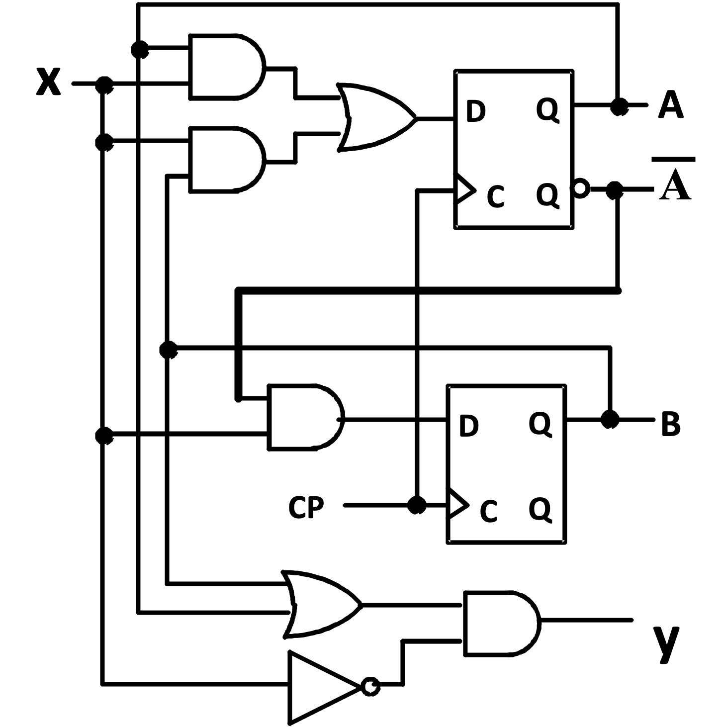
- Current State: \(A, B\)
- Next State: \(A(t+1) = AX + BX, B(t+1) = \bar AX\)
- Output: \(Y = (A + B)\bar X\)
State Table
A multiple variable table with the following four sections:
- Present State: the values of the state variables for each allowed state.
- Inputs: the input combinations allowed
- Next state: the value of the state at time (t+1) based on the present state and the input.
- Outputs: the value of the output as a function of the present state and (sometimes) the input.
Example
上一例中的电路图的状态表:

或者写成:

State Diagrams
The sequential circuit function can be represented in graphical form as a state diagram.
Label form:
- On circle with output included:
- state/output
- Moore type output depends only on state
- On directed arc with the output included:
- input/output
- Mealy type output depends on state and input
Example

Equivalent State Definitions
Two states are equivalent if their outputs produced for each input symbol is identical and their next states for each input symbol are the same or equivalent.
若两个状态接受相同输入后输出相同,且下一个状态相同或等价,则两个状态等价。
Example

图中 S1、S2、S3 等价,可以写成一个状态:

Moore and Mealy Models
Sequential Circuits or Sequential Machines are also called Finite State Machines (FSMs). Two formal models exist:
-
Moore Model: the outputs depend only on the present state.
State Diagram 中,输出写在状态节点上。
-
Mealy Model: the outputs depend on the present state and the inputs.
State Diagram 中,输出写在状态转移边上。
Flip-Flop Timing Parameters
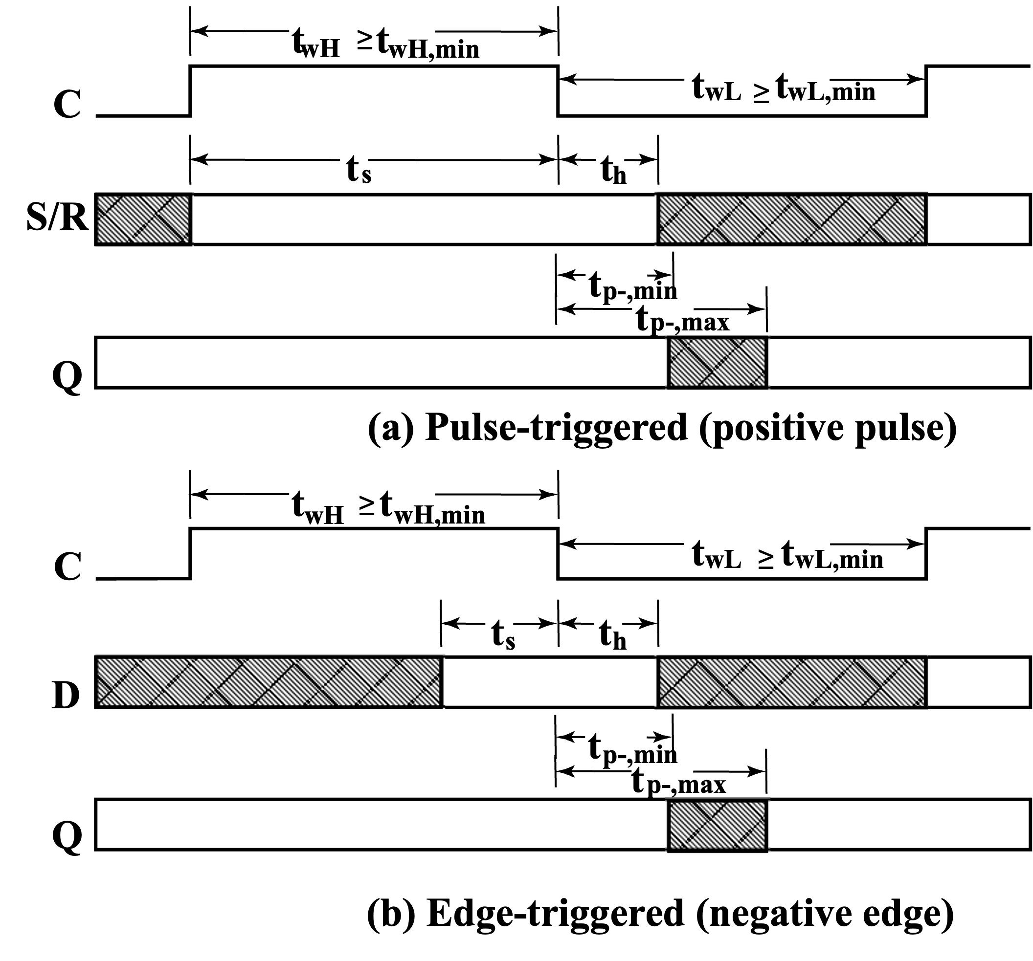
- \(t_s\): setup time 准备时间,在状态进行更新之前需要准备好
- \(t_h\): hold time 一般为 0,保持时间,在状态更新之后需要保持一段时间
- \(t_w\): clock pulse width, usually \(t_{wH} = t_{wL}\)
- \(t_{px}\): propagation delay
- \(t_{PHL}\): High-to-Low
- \(t_{PLH}\): Low-to-High
- \(t_{pd}\): \(\max(t_{PHL}, t_{PLH})\)
Circuit and System Level Timing

计算触发器从输出到输入的延迟,可以将出发器的输出和输入拆开,更加直观地计算延迟。
If the clock period is too short, some data changes will not propagate through the circuit to flip-flop inputs before the setup time interval begins.
New timing components:
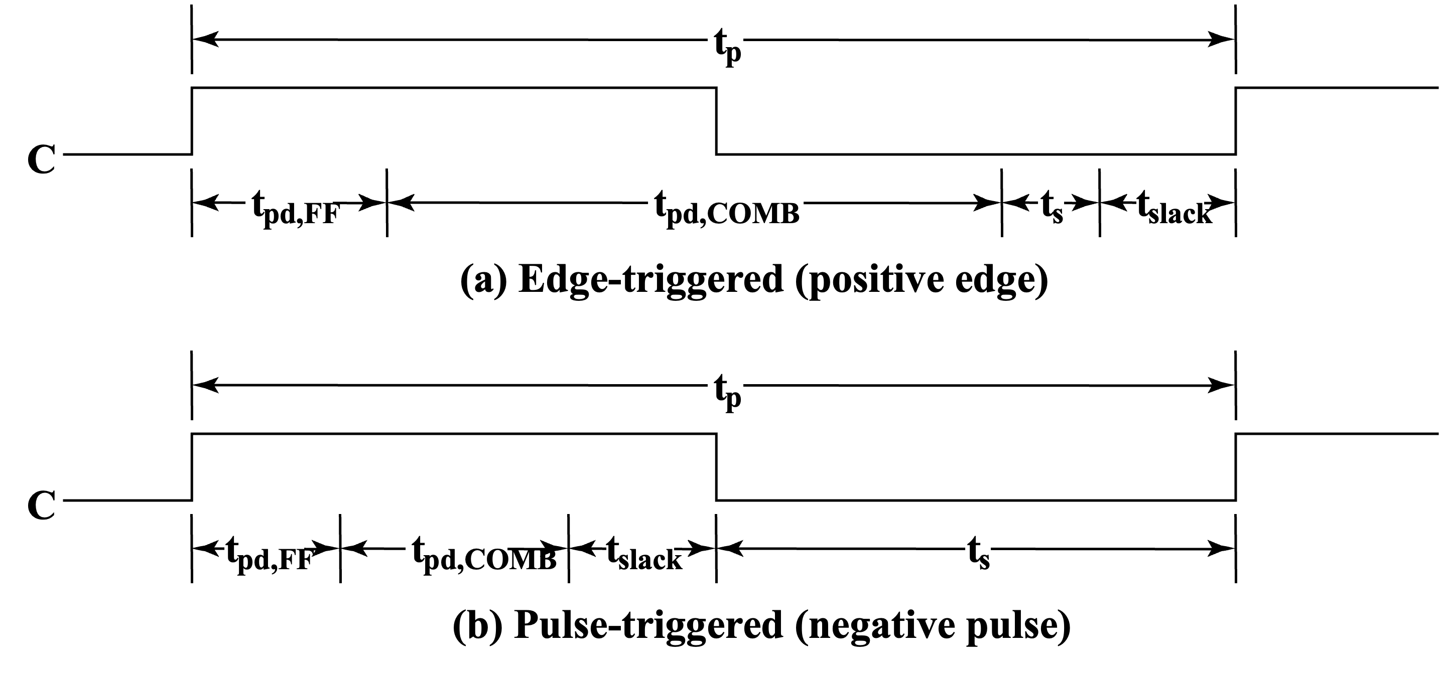
- \(t_p\): clock period 时钟周期
- \(t_{pd,COMB}\): total delay of combinational logic along the path from flip-flop output to flip-flop input
- \(t_{slack}\): extra time in the clock period in addition to the sum of the delays and setup time on a path
降低延迟:主要考虑优化 \(t_{pd,COMB}\),减少组合逻辑的延迟。
Time equation
for all paths from flip-flop output to flip-flop input.
Example
- \(t_{pd,FF} = 1.0 ns\)
- \(t_s = 0.3 ns\) for edge-triggered flip-flops
- \(t_s = t_{wH} = 2.0 ns\) for master-slave flip-flops
- Clock frequency = 250 MHz
Calculations:
\(t_p = 1 / 250 MHz = 4.0 ns\)
-
Edge-triggered: \(4.0 \geq 1.0 + t_{pd,COMB} + 0.3 \Rightarrow t_{pd,COMB} \leq 2.7 ns\)
Approximately 9 gates allowed on a path
-
Master-slave: \(4.0 \geq 1.0 + t_{pd,COMB} + 2.0 \Rightarrow t_{pd,COMB} \leq 1.0 ns\)
Approximately 3 gates allowed on a path
Sequential Circuit Design
The Design Procedure:
- Specification
- Formulation: Obtain a state diagram or state table
- State Assignment: Assign binary codes to the states
- Flip-Flop Input Equation Determination
- Output Equation Determination
- Optimization
- Technology Mapping
- Verification
Specification
Component Forms of Specification
- State Diagram
- State Equations
- HDL codes
- ...
Formulation
A state is an abstraction of the history of the past applied inputs to the circuit.
触发器数量选择:\(n = \lceil \log_2 m \rceil\),\(m\) 为状态数。
Sequence Recognizer Procedure 序列识别器
用处:识别输入序列(比如识别通信序列中的开始和结束)。
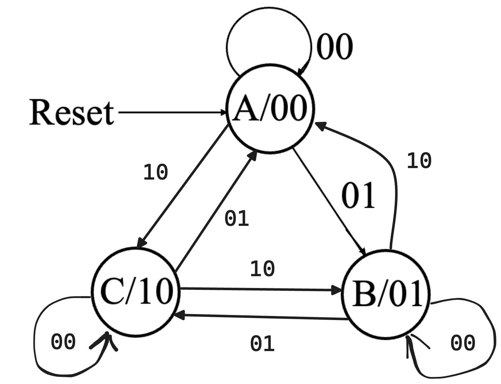
Example: Recognize the sequence 1101.
-
识别 1101:

-
考虑所有可能的输入序列:

-
得到状态表

上述过程是 Mealy Model,如果是 Moore Model,则还需要增加一个状态:

Simplification of State Diagrams
一般情况下,原始状态图和原始状态表中存在着多余的状态。状态个数越多,电路中所需的触发器的数目也越多,制造成本就越高。为降低制造成本,需要去掉多余的状态。
所谓状态简化,就是要获得一个最小化的状态表。这个表不仅能正确地反映设计的全部要求,而且状态的数目最少。
状态等效:对于所有可能的输入序列,两个状态的输出序列相同,且下一个状态相同或等效,则两个状态等效,可以合并。
状态等效判别:
首先输出相同,同时满足以下三个条件之一:
- 次态相同
- 次态交错
- 次态循环
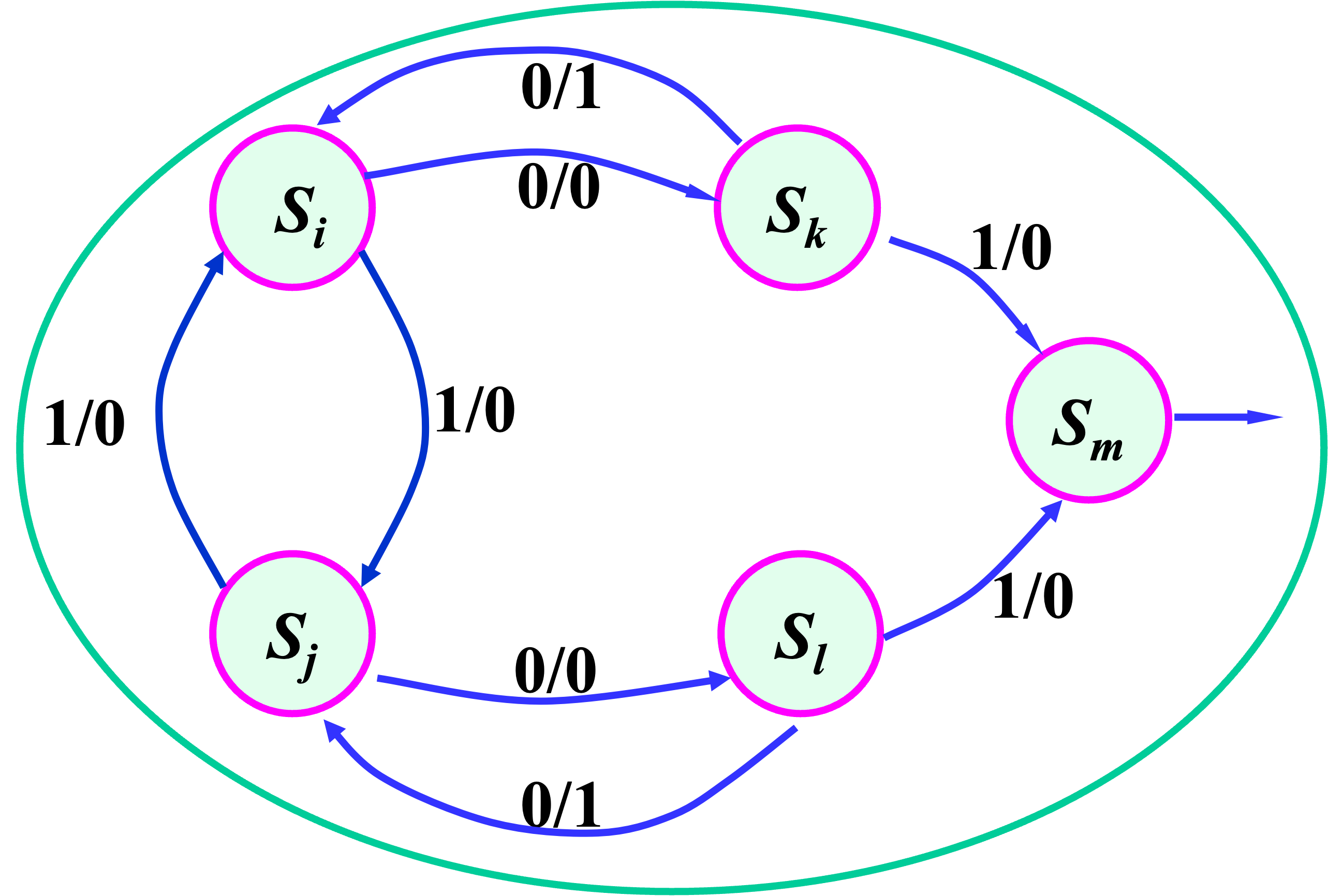
Example
-
次态相同
-
次态相同或交错
-
次态相同或等效(\(S_k, S_l\) 等效)
-
次态交错或相同或循环
化简方法:
-
观察法化简
从状态图/状态表中观察出等效状态,然后合并。
-
隐含表法化简
状态 \(S_1, \dots, S_n\),作 \((n-1) \times (n-1)\) 的梯形图,列分布代表 \(S_1, \dots, S_{n-1}\),行分别代表 \(S_2, \dots, S_n\), 每个格子代表 \(S_i, S_j\) 的次态是否相同,若无法确定,则写上依赖的状态对。可以容易地看出依赖关系,从而进行化简。
Example
化简:

画出隐含表:
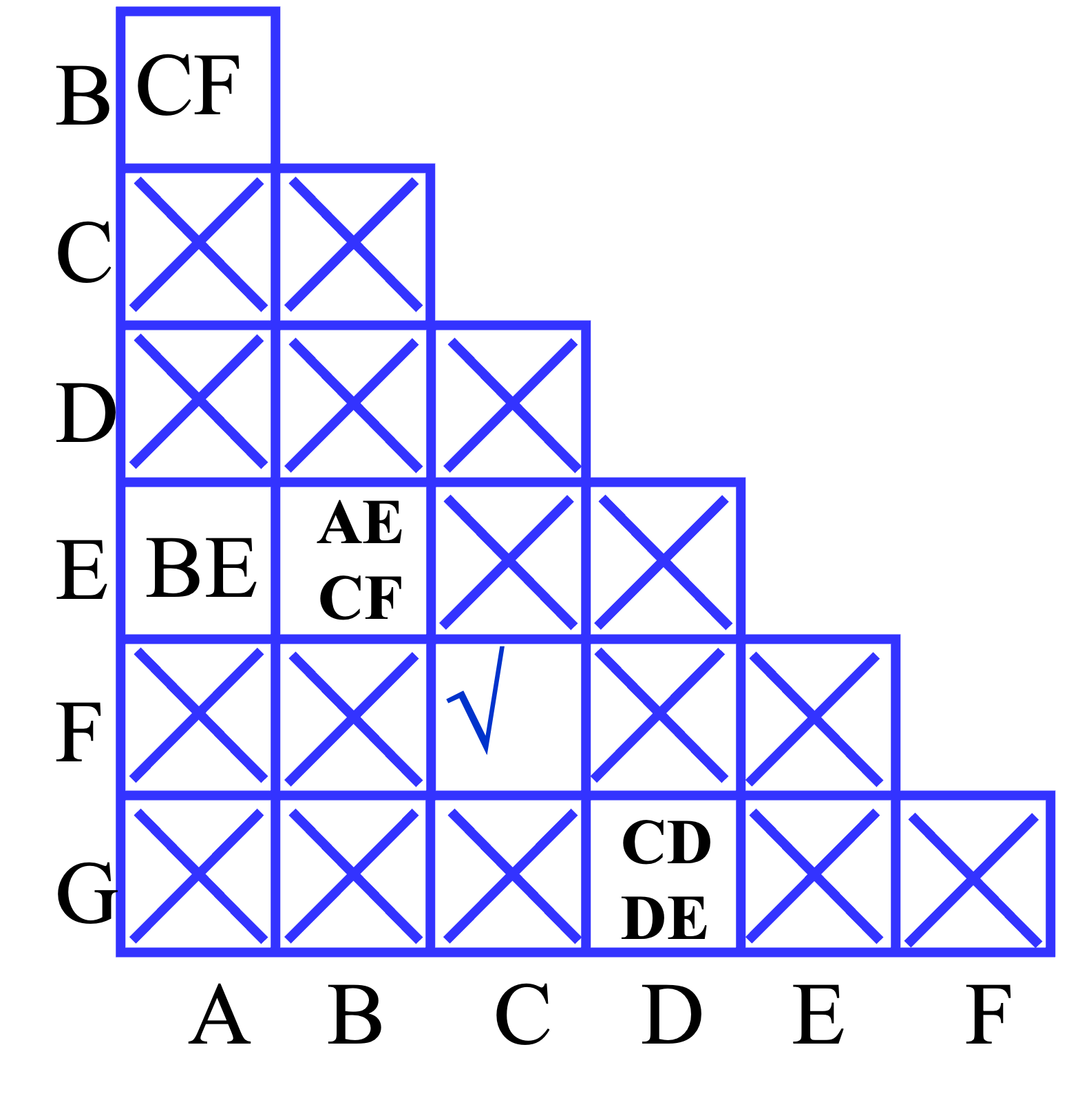
可以看出:
- \(AB \rightarrow CF \rightarrow equivalent\)
- \(AE \leftrightarrows BE \rightarrow CF \rightarrow equivalent \Rightarrow ABE \rightarrow equivalent\)
确定最大等效类,作最小化状态表:
- 四个等效对 \((A,B), (A,E), (B,E), (C,F)\)
- 最大等效类 \((A,B,E)\)
- 四个状态 \((A,B,E), (C,F), (D), (G)\)
令以上四个状态依次为 \(a, b, c, d\),画出最小化状态表:

State Assignment
If the number of states is \(m\), then \(n = \lceil \log_2 m \rceil\) bits are required to represent the states.
There are \((2^n)!/m!\) assignments of codes with a minimum number of bits.
Find Flip-Flop Input and Output Equations
Use K-maps to compute the equations of \(D_i, X_{output}\) with respect to \(X_{input}, Q_i\).
通常情况下,状态分配的方案不一样,所得到的输出函数和激励函数的表达式也不同,由此而设计出来的电路复杂度也不同。
实际应用时都是采用工程近似的方法,依据以下四条件原则来进行状态分配:
- 在相同输入条件下具有相同次态的现态,应尽可能分配相邻的二进制代码
- 在相邻输入条件,同一现态的次态应尽可能分配相邻的二进制代码
- 输出 完全相同 的现态应尽可能分配相邻的二进制代码
- 最小化状态表中出现次数最多的状态或初始状态应分配逻辑
0
一般情况下,第一条原则较为重要,需优先考虑,其次要考虑由前三条原则得到的应分配相邻代码的状态对出现的次数,次数多的状态对应优先分配相邻的二进制代码。
Example
对下列状态表进行状态分配:

- 在相同输入条件下具有相同次态的现态,应尽可能分配相邻的二进制代码:A 和 B,A 和 C 应相邻
- 在相邻输入条件,同一现态的次态应尽可能分配相邻的二进制代码:C 和 D,C 和 A,B 和 D,A 和 B 应相邻
- 输出完全相同的现态应尽可能分配相邻的二进制代码: A,B,C 三者应相邻,即 A 和 B,A 和 C,B 和 C应相邻
- 最小化状态表中出现次数最多的状态或初始状态应分配逻辑 0:A 分配为逻辑 0
由此得到状态分配方案:

Sequential Design Example
Design a sequential modulo 3 accumulator for 2-bit operands.
- Modulo n adder: an adder that gives the result of the addition as the remainder of the sum divided by n.
- Accumulator: a circuit that "accumulates" the sum of its input operands over time - it adds each input operand to the stored sum, which is initially 0.
Stored sum: \((Y_1, Y_0)\). Input: \((X_1, X_0)\). Output: \((Z_1, Z_0)\)
State diagram:
State table:

State assignment \(\to\) Flip-flop input equations.
Other Flip-Flop Types
J-K Flip-flop
Similar to SR flip-flop, but without the invalid state.
\(J = K = 1\) 时,状态求反。
主从触发器实现,有 1s catching 问题。
用 D 触发器实现,避免 1s catching 问题:
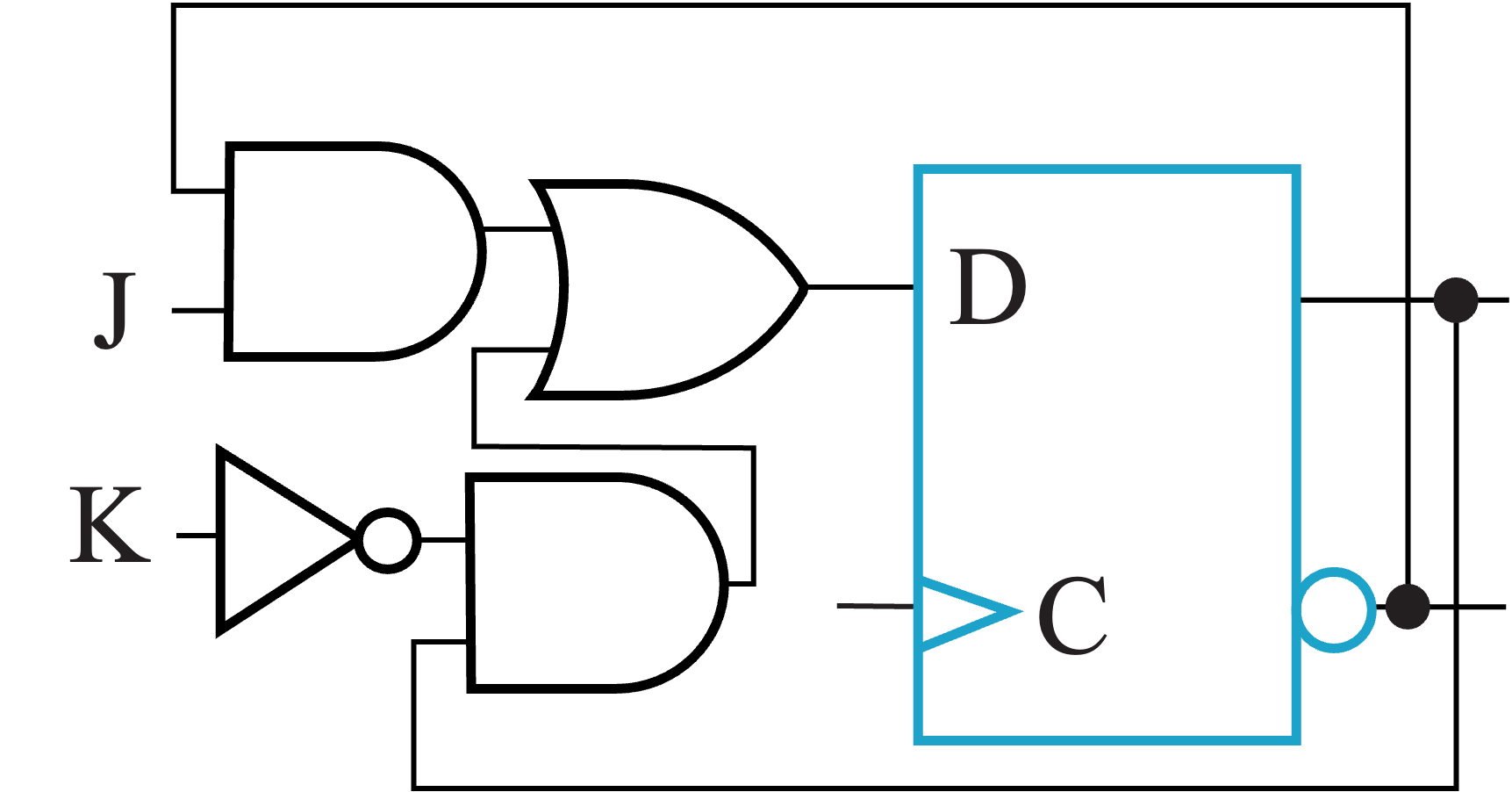
上升沿触发。
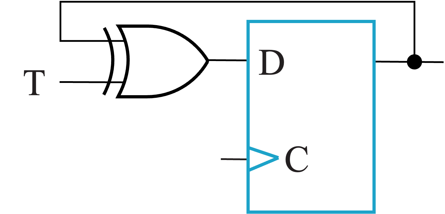
T Flip-flop
- For \(T = 0\), no change in state
- For \(T = 1\), changes to opposite state
Same as a J-K flip-flop with \(J = K = T\)
一般会强制设置初态。
用 D 触发器实现:
Basic Flip-Flop Descriptors
Used in analysis:
- characteristic table 特征表: defines the next state of the flip-flop in terms of flip-flop inputs and current state
- characteristic equation 特征方程: defines the next state of the flip-flop as a Boolean function of flip-flop inputs and current state
Used in design:
- excitation table 激励表: defines the flip-flop input variable values as function of the current state and next state
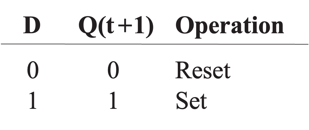
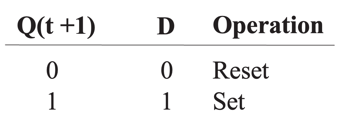
D Flip-Flop Descriptors
Characteristic table:
Characteristic equation:
Excitation table:
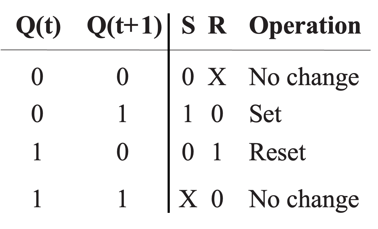
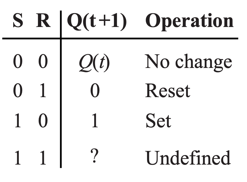
S-R Flip-Flop Descriptors
Characteristic table:
Characteristic equation:
Excitation table: