Memory Basics
Memory Definitions
-
Memory: A collection of storage cells together with the necessary circuits to transfer information to and from them.
一组存储单元的集合,可以读、写。
-
Memory Organization: The basic architectural structure of a memory in terms of how data is accessed.
内存的架构,内存能存放多少数据,一个字多少位,如何访问内存等。
-
Random Access Memory (RAM): A memory organized such that data can be transferred to or from any cell (or collection of cells) in a time that is not dependent upon the particular cell selected.
-
Memory Address: A vector of bits that identifies a particular memory element (or collection of elements).
内存地址,一个列表的编号,通过编号可以读写内存的数据。
-
Typical data elements:
- Bit: A single binary digit (0 or 1).
- Byte: A group of 8 bits.
-
Word: A group of bits that is treated as a unit by the computer hardware.
一次读写的数据单元,一般为 8 位或 16 位。
-
Memory Data: a bit or a collection of bits to be stored into or accessed from memory cells.
写入或读取的数据。
-
Memory Operations: operations on memory data supported by the memory unit.
Memory Organization
Organized as an indexed array of words. Value of the index for each word is the memory address.
Memory Block Diagram
A basic memory system is shown here 基础的内存系统:

- k address lines are decoded to address \(2^k\) words of memory.
- Each word is n bits.
- Read and Write are single control lines defining the simplest of memory operations.
Memory Operations
Memory operations require the following:
- Data: data written to, or read from, memory as required by the operation. 输入或输出的数据。
-
Address: specifies the memory location to operate on. The address lines carry this information into the memory.
Typically: n bits specify locations of \(2^n\) words.
-
An operation: Information sent to the memory and interpreted as control information which specifies the type of operation to be performed. 控制信号,指定操作类型。
Typically: a single bit specifies READ or WRITE.
-
Read Memory: an operation that reads a data value stored in memory:
读取内存中的数据。
- Place a valid address on the address lines.
- Toggle the memory read control line.
- Wait for the read data to become stable.
-
Write Memory: an operation that writes a data value to memory:
写入数据到内存。
- Place a valid address on the address lines and valid data on the data lines.
- Toggle the memory write control line.
-
Memory Operation Timing
Most basic memories are asynchronous
-
Read Timing
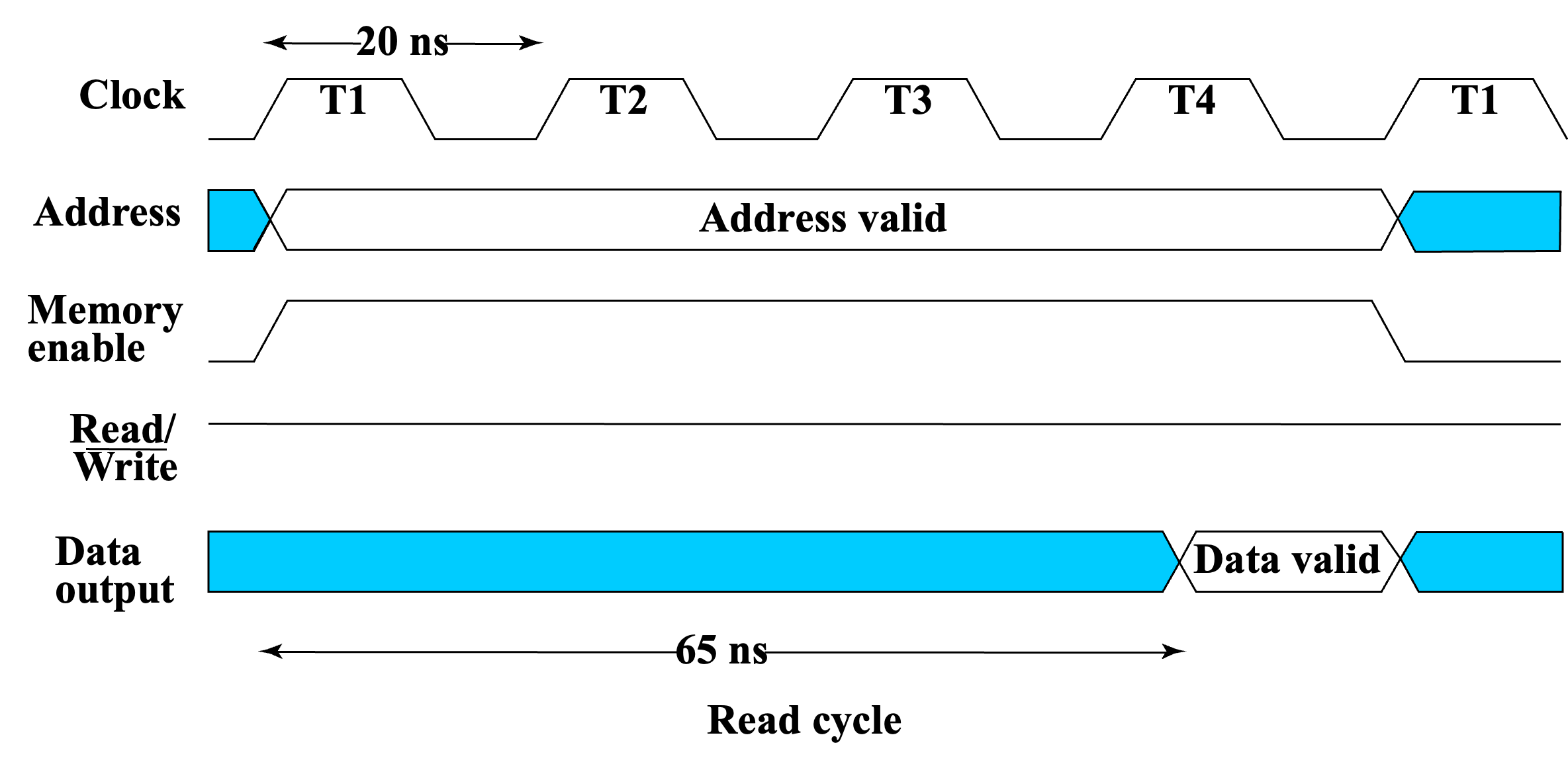
data valid之前需要等待一段时间,因为内存需要一定的时间读取数据。这个时间取决于内存的速度。 -
Write Timing
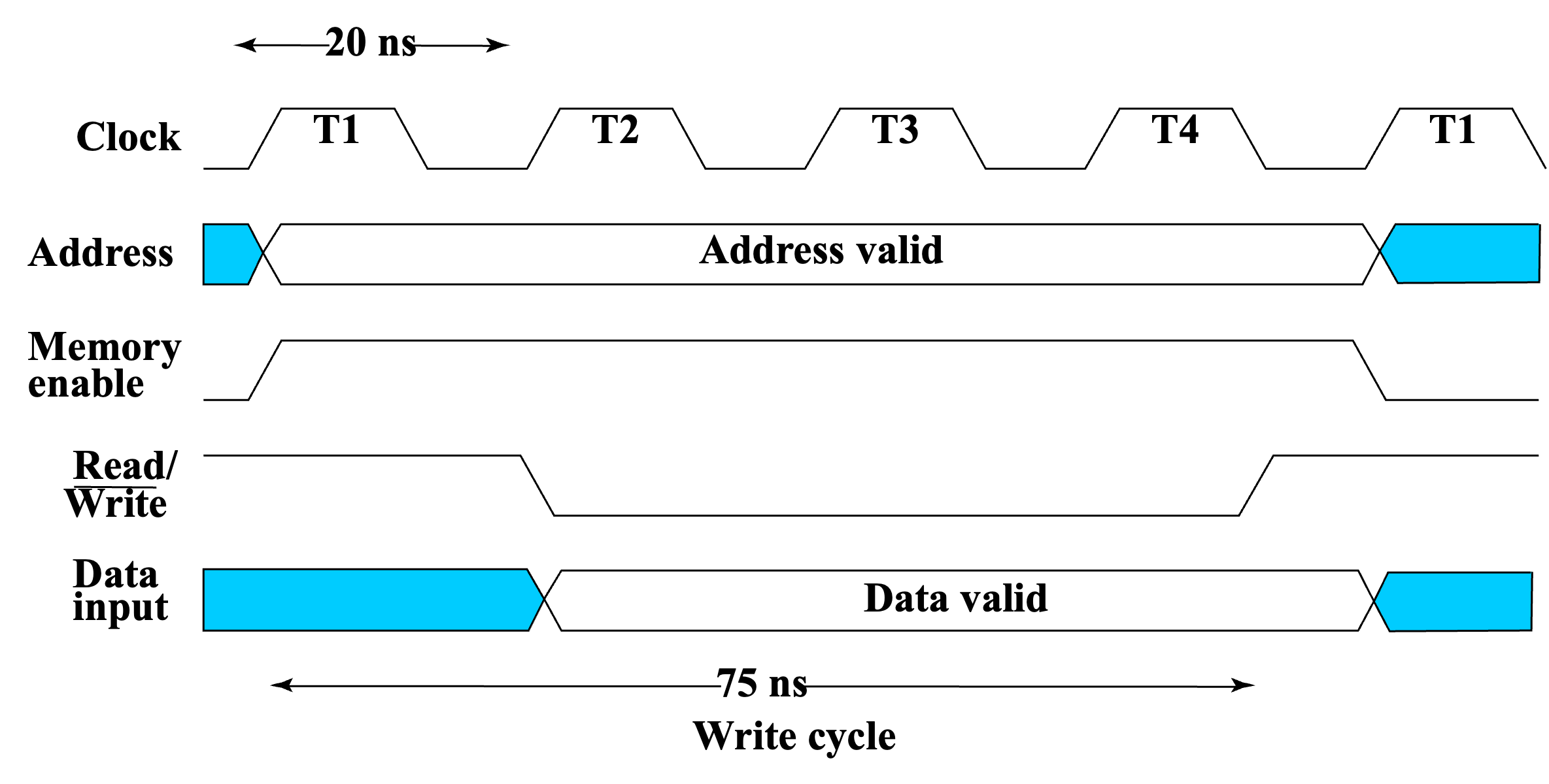
在 R/W 信号下降时要将 addr 锁存起来,上升时要预先把数据准备好。
RAM Integrated Circuits
Types of random access memory:
-
Static RAM (SRAM): information stored in latches
信息存储在锁存器中,不需要刷新。
-
Dynamic RAM (DRAM): information stored as electrical charges on capacitors
信息存储在电容中,需要刷新。
- Charge "leaks" off: 电容会漏电
- Periodic refresh of charge required: 需要定期刷新
Dependence on Power Supply:
- Volatile: loses stored information when power turned off. 掉电后会丢失数据。
- Non-volatile: retains information when power turned off. 掉电后不会丢失数据。
Address bus and Data bus: 数据总线和地址总线
- Address bus: 传输地址,\(存储容量=2^{地址总线位数}\)
- Data bus: 传输数据,\(一次处理数据的位宽=数据总线位数\)
Static RAM
Storage Cell
-
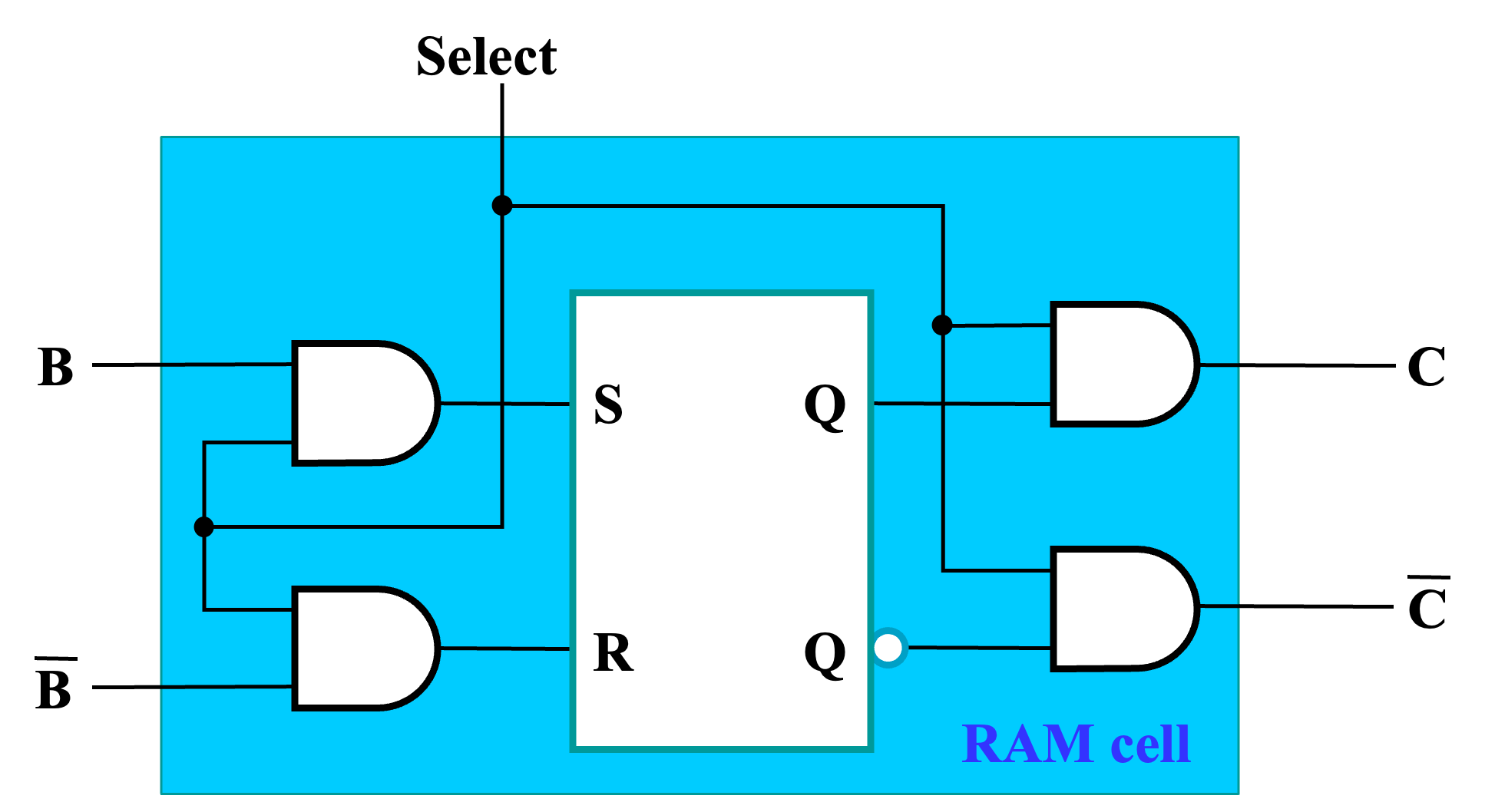
SR Latch: stores one bit of information
一个锁存器,存储一位信息。
-
Select: select input for control
控制信号,控制读写。如果为 1,那么数据会被写入到锁存器中。如果为 0,那么锁存器的值不会被修改和读出。
-
Dual Rail Data Inputs \(B\) and \(\bar B\): dual rail 数据输入
- Dual Rail Data Outputs \(C\) and \(\bar C\): dual rail 数据输出
Bit Slice
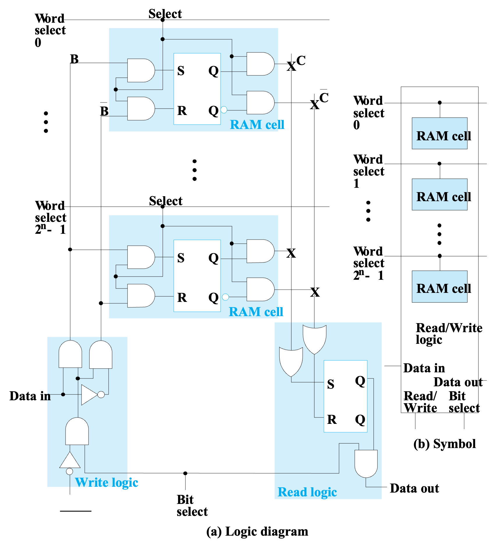
Bit Select: 控制整个 bit slice 的工作,当 Bit Select 为 0 时,整个 bit slice 不工作;当 Bit Select 为 1 时,bit slice 的读写收 Read/Write 控制。
当 Bit Select 为 1 时:
- Read Operation: Read/Write 为 1,此时 Data in 处与门不工作,锁存器保持原来的值。根据 Word Select 选择输出的数据。
- Write Operation: Read/Write 为 0,此时 Data in 处与门工作,根据 Word Select 选择写入的数据。
Cell Arrays and Coincident Selection
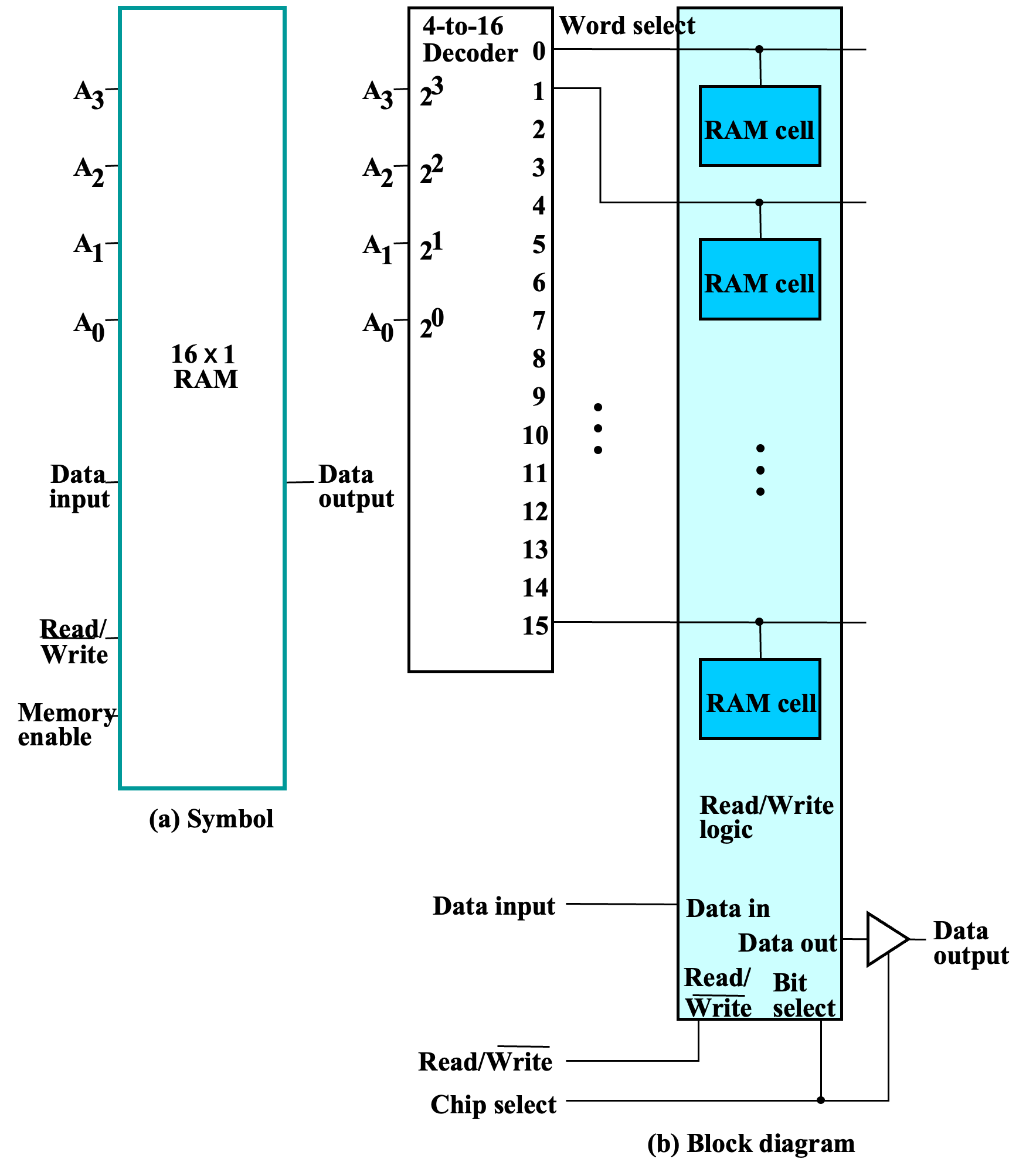
- Decoder: 译码器,将地址译码为控制信号,将对应地址上 RAM cell 的 Select 置为 1。
- 三态门:使得 RAM chip 的输出可以与总线连接。
行列译码
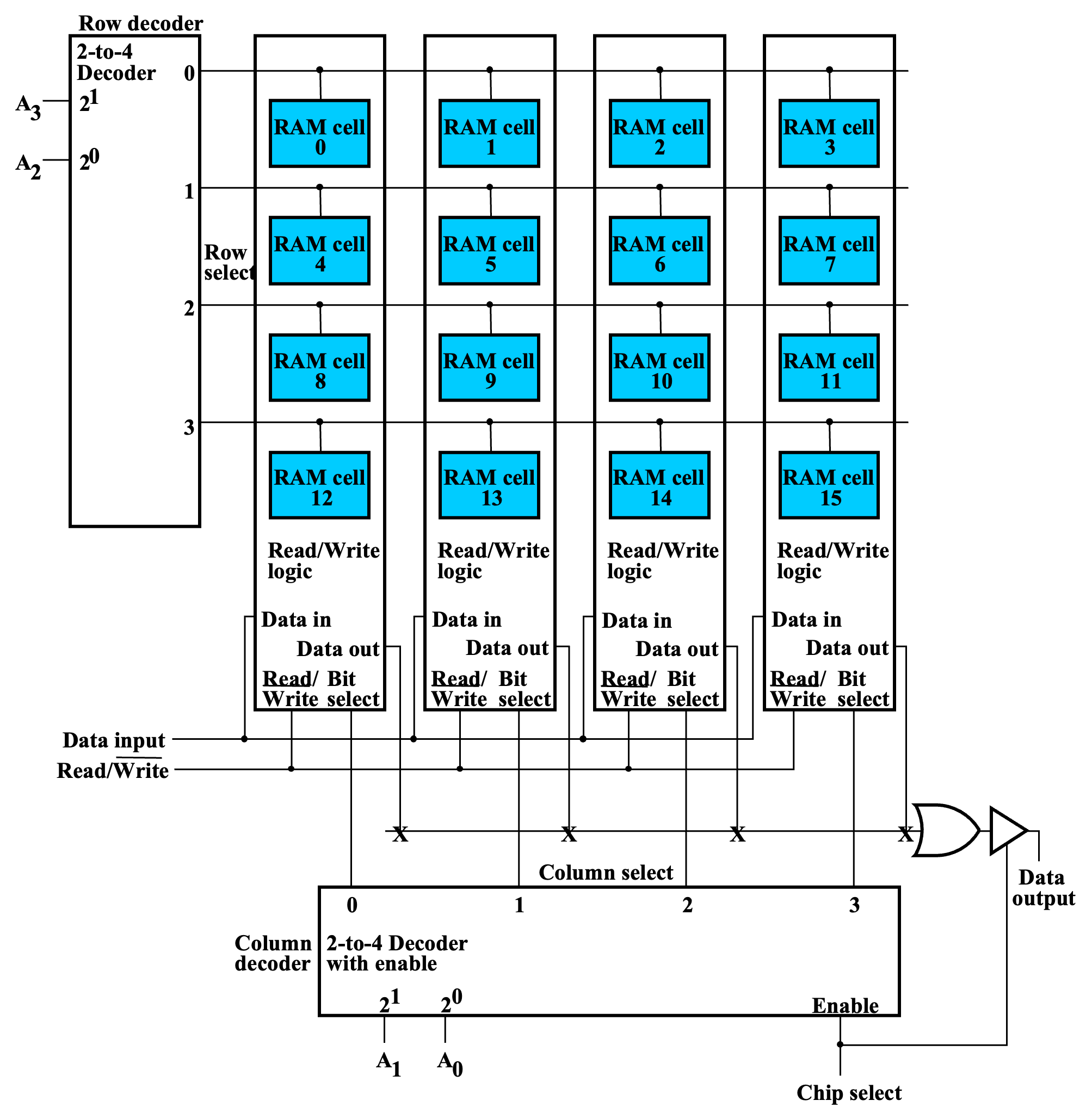
\(8\times 2\) RAM
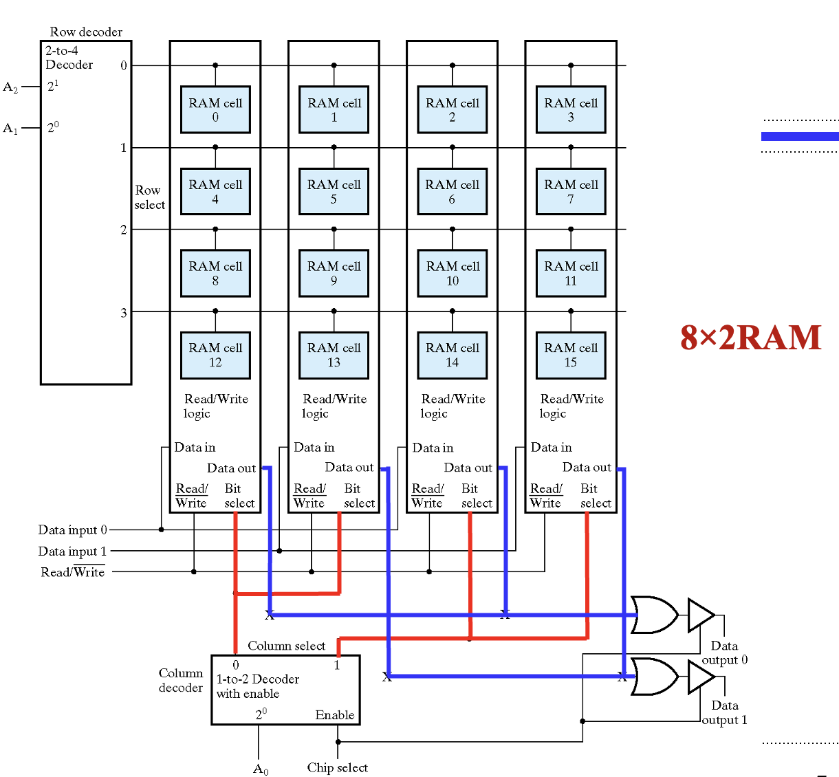
RAM slice 0 和 2、1 和 3 作为数据的高低位。
Making Larger Memories

高两位接入译码器,低两位接入 RAM chip,减少复杂度。
Making Wider Memories

增加位宽,每块 RAM chip 就代表最后输出的某一位。
Dynamic RAM
Basic Principle: Storage of information on capacitors. 信息存储在电容上。
DRAM Cell
- Capacitor: 电容
- Switch: 开关
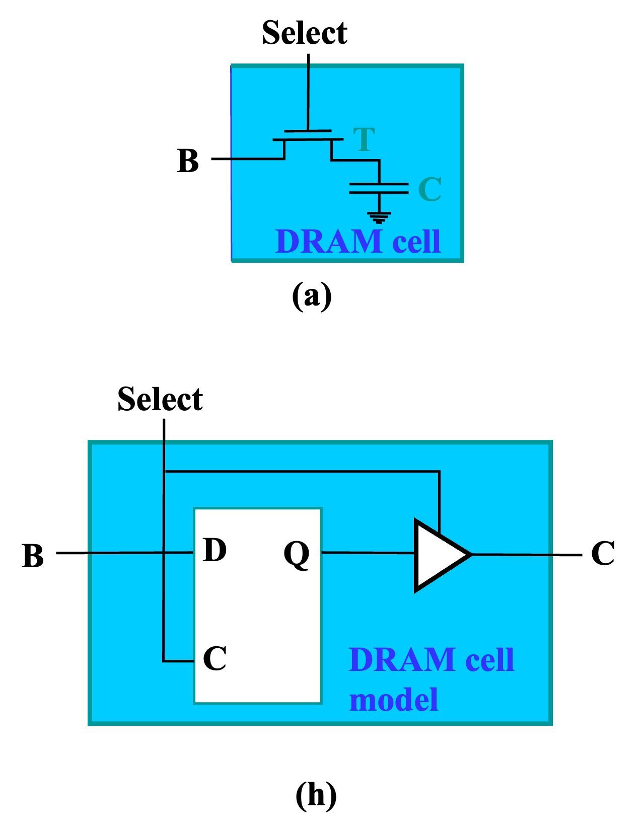
基本功能:
- Store: 用三态门将电容锁住。
- Write: 将电容充电或放电。
- Read: 读取电容的电压。
DRAM Slice
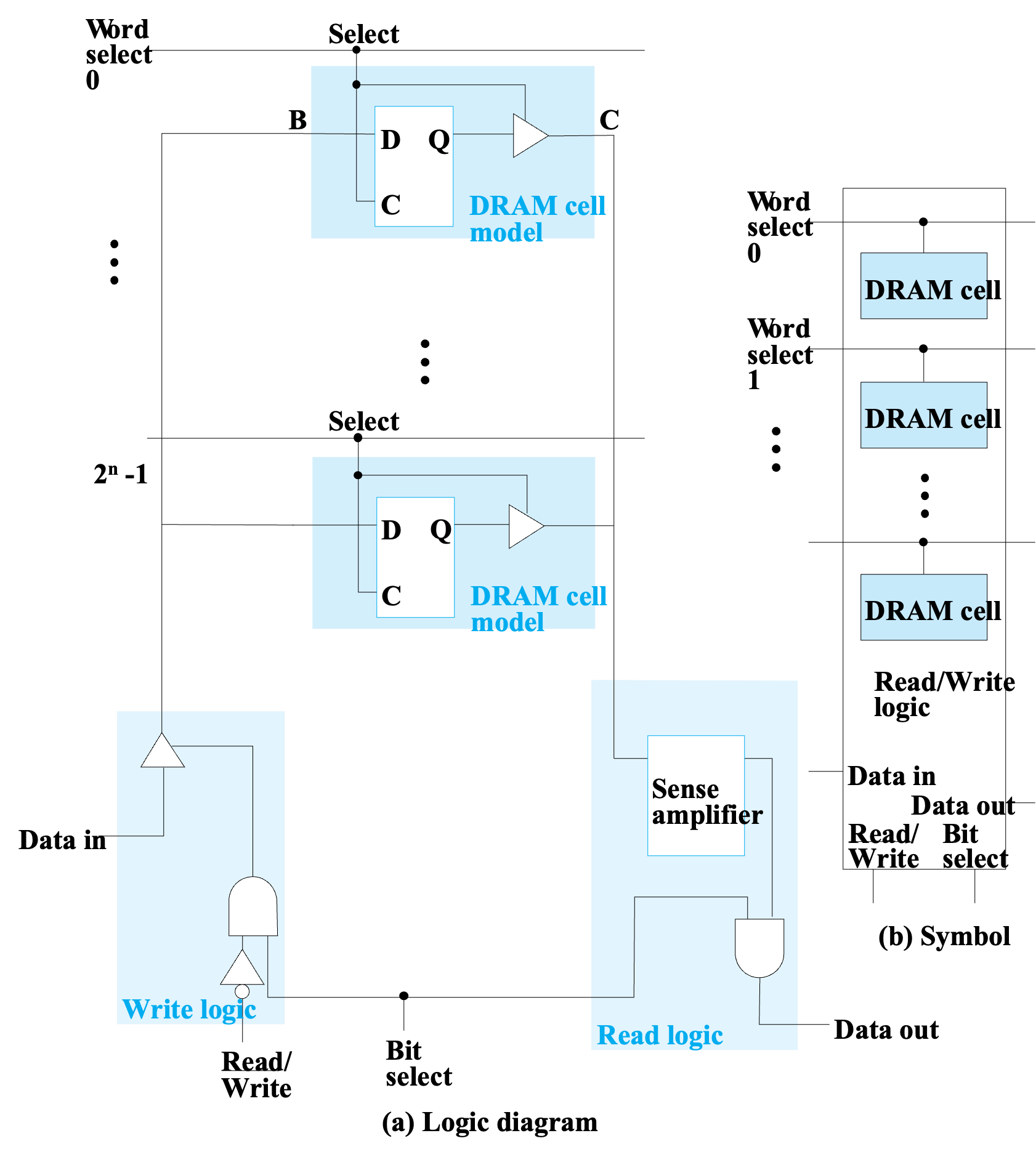
Block Diagram
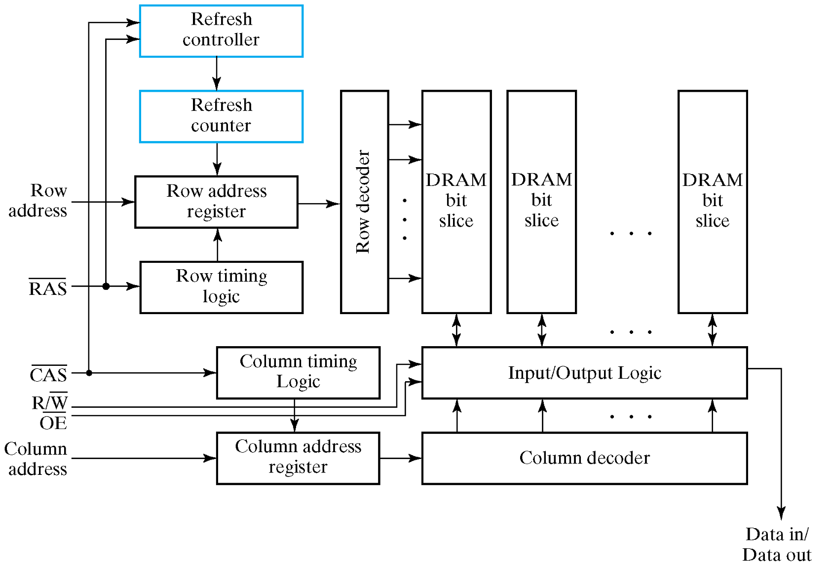
Read and Write Operations: 分开读取行列地址,CPU 提供信号告诉 DRAM 当前读取的是行地址还是列地址。
-
Application of row address: \(\overline{RAS}\)
读取行地址,将行地址放入译码器,将对应的行的电容放入读取电路。
-
Application of column address: \(\overline{CAS}\)
读取列地址,将列地址放入译码器,将对应的列的电容放入读取电路。
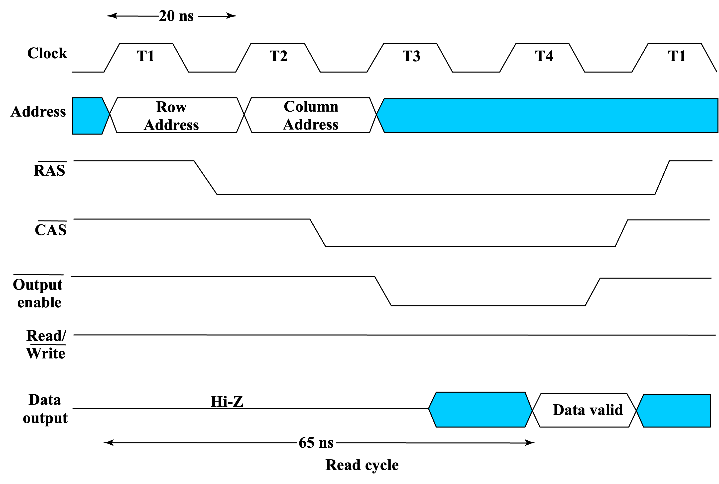
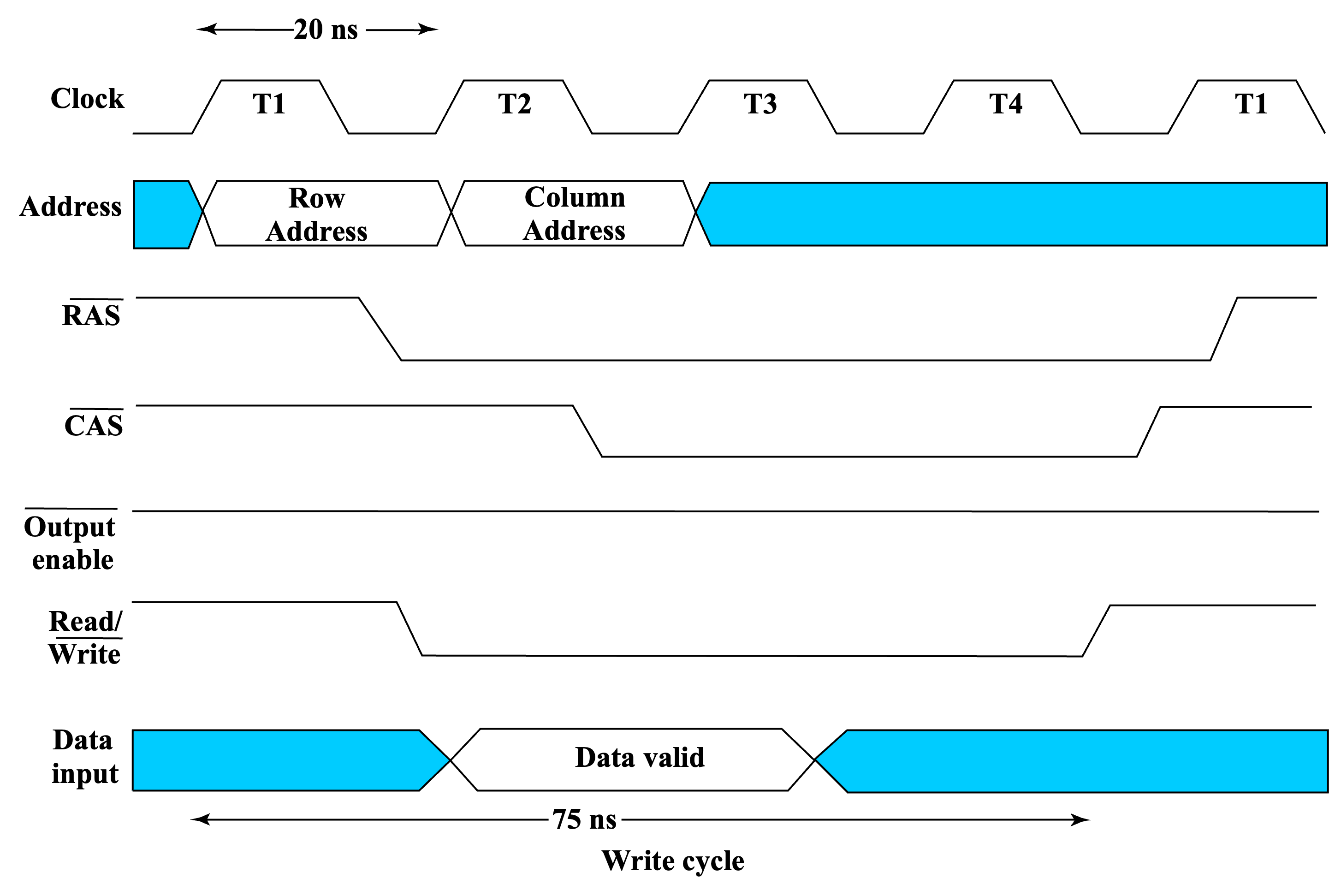
Dynamic RAM Timing
-
Read Timing
-
Write Timing
DRAM Types
- Synchronous DRAM (SDRAM)
- Double Data Rate SDRAM (DDR SDRAM)
- RAMBUS® DRAM (RDRAM)
Synchronous DRAM:
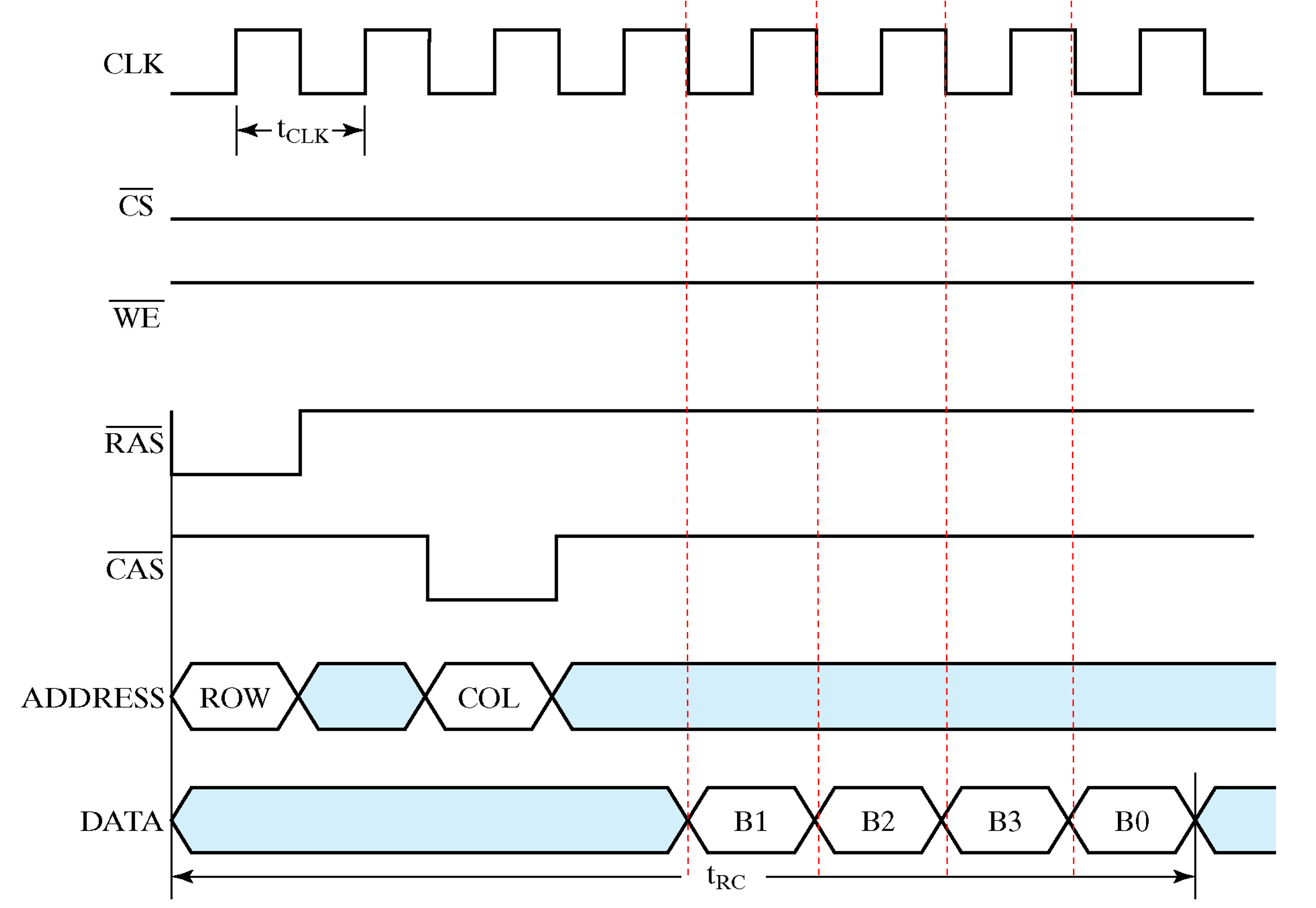
Transfers to and from the DRAM are synchronize with a clock。
有时钟,一次可以读出多个数据。
Synchronous DRAM - burst size=4
Double Data Rate SDRAM:
Transfers data on both edges of the clock. 在时钟的上升沿和下降沿都可以读出数据。
Provides a transfer rate of 2 data words per clock cycle.
RAMBUS® DRAM:
Uses a packet-based bus for interaction between the RDRAM ICs and the memory bus to the processor.
The bus consists of:
- A 3-bit row address bus
- A 5-bit column address bus
- A 16 or 18-bit (for error correction) data bus
使用包传输,一次可以读出多个数据。